L03 · Pipelining
L03 · Pipelining
Topic: pipelining · 47 pages
EECS 4340 Lecture 3 — Basic Pipelining

Announcements

Show slide text
Announcements
- Lab #2 this Wednesday
- Please bring your computer
- Involve graded assignments
- Attendance is required and graded
- Project #1
- Due 4-Feb-26
- Project #2
- Will be released today (2-Feb-26)
- Due 11-Feb-26
- More details in the lab
Readings
Show slide text
Readings
For today:
- H & P Chapter C.1–C.4
Recap: Performance & Power
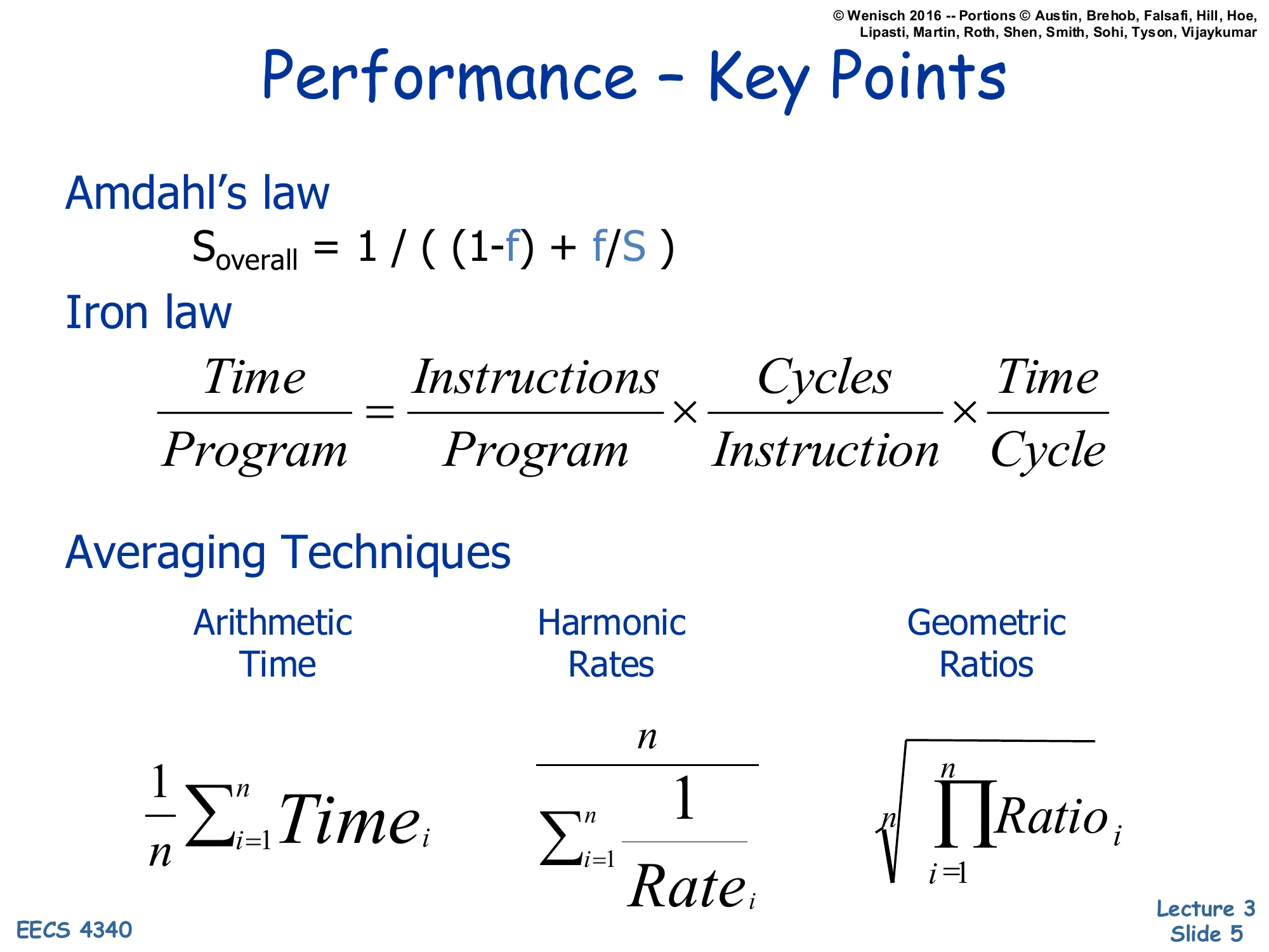
Performance — Key Points
Show slide text
Performance — Key Points
Amdahl’s law
Soverall=(1−f)+f/S1
Iron law
ProgramTime=ProgramInstructions×InstructionCycles×CycleTime
Averaging Techniques
- Arithmetic (Time): n1∑i=1nTimei
- Harmonic (Rates): ∑i=1nRatei1n
- Geometric (Ratios): n∏i=1nRatioi
This recap consolidates three pieces of L02 that you need before pipelining makes sense. Amdahl’s law bounds total speedup when only a fraction f of execution is improved by factor S — even a perfectly parallel speedup of the parallelizable fraction leaves the serial (1−f) part as a hard floor. The Iron Law decomposes program execution time into three multiplicative terms — dynamic instruction count, cycles per instruction, and cycle time — so every architectural change can be classified by which term it changes. Pipelining, the topic of this lecture, primarily attacks the cycle time factor (by shortening each stage) while attempting to keep IPC near 1. The averaging slide reminds you that different metrics need different means: arithmetic mean is correct for raw times, harmonic mean is correct for rates (because 1/x=1/xˉ), and geometric mean is the only sensible choice for normalized ratios — averaging speedup ratios with arithmetic mean exaggerates whichever baseline is in the denominator.
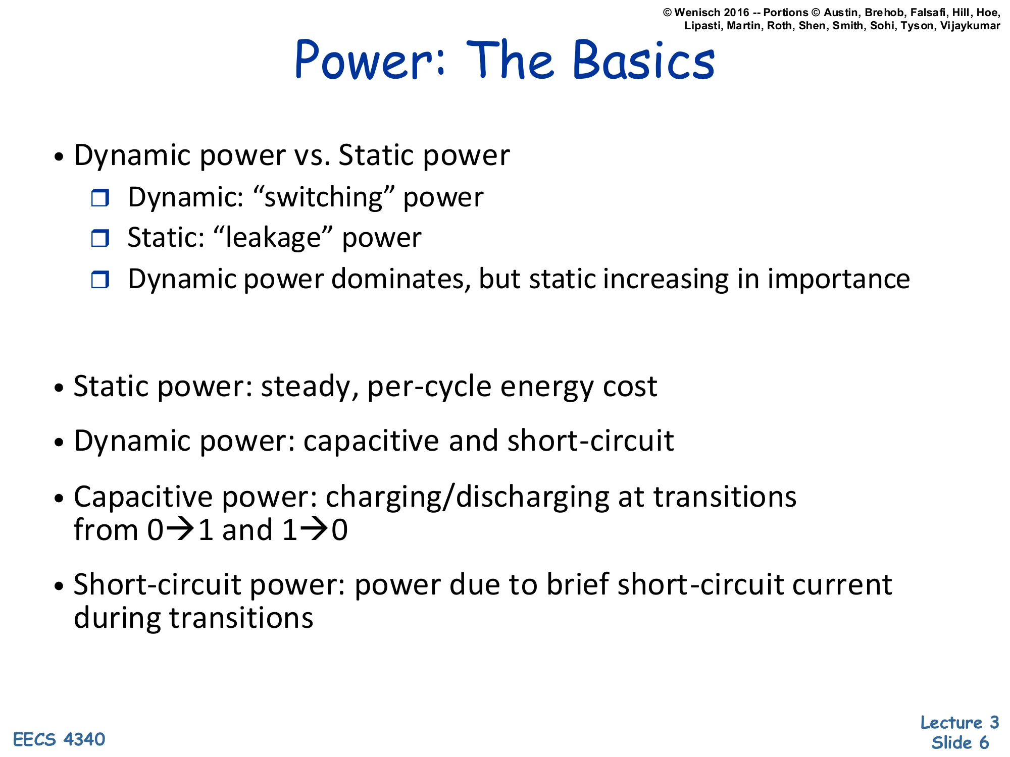
Power: The Basics
Show slide text
Power: The Basics
- Dynamic power vs. Static power
- Dynamic: “switching” power
- Static: “leakage” power
- Dynamic power dominates, but static increasing in importance
- Static power: steady, per-cycle energy cost
- Dynamic power: capacitive and short-circuit
- Capacitive power: charging/discharging at transitions from 0→1 and 1→0
- Short-circuit power: power due to brief short-circuit current during transitions
CMOS chips dissipate power in two regimes. Dynamic power scales with how often nodes toggle and with how much voltage they swing; it is the cost of doing computation. Static (leakage) power flows whenever the chip is on, even with no activity, because real transistors are imperfect switches. Historically dynamic power dominated, but as feature sizes shrank into deep sub-micron, leakage grew because the threshold voltage Vt had to be lowered to keep Vdd scaling viable, and subthreshold conduction grows exponentially as Vt drops. Within dynamic power there are two sub-components: capacitive switching power, the energy needed to charge a wire’s load capacitance from 0 to Vdd (or discharge it back), and short-circuit power, the very brief NMOS-and-PMOS-both-conducting current spike during the transition itself. The first term is the one architects can control through the 21CV2Af relation introduced on the next slide.
Capacitive Power Dissipation
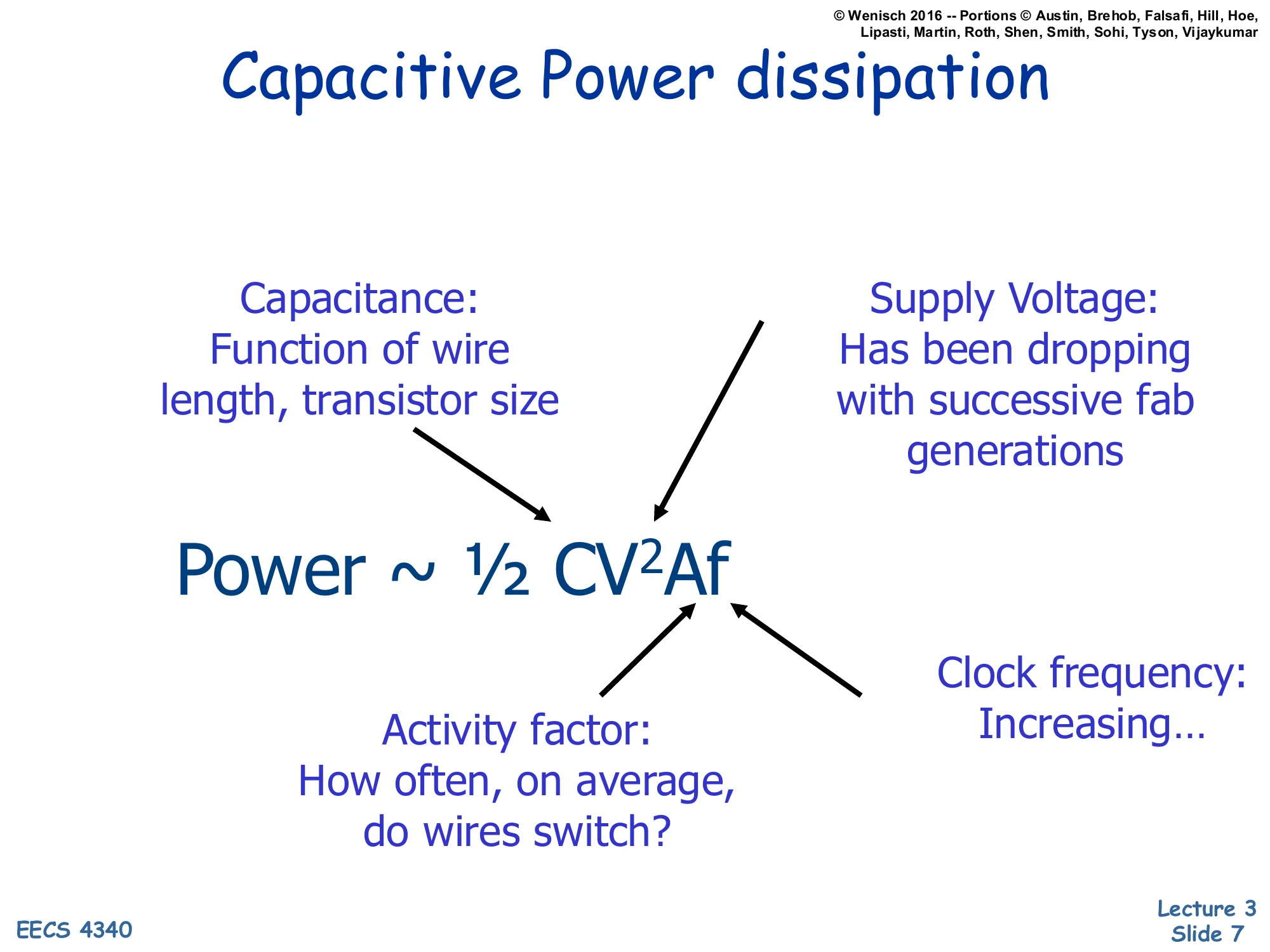
Show slide text
Capacitive Power Dissipation
P∼21CV2Af
- Capacitance (C): function of wire length, transistor size
- Supply Voltage (V): has been dropping with successive fab generations
- Activity factor (A): how often, on average, do wires switch?
- Clock frequency (f): increasing…
The 21CV2Af equation is the architect’s lever for dynamic power. Each time a node toggles it dumps energy 21CV2 into heat, the activity factor A converts “per-toggle” energy into average switching events per cycle, and the clock f converts cycles into seconds. The four knobs are not independent: shrinking transistors reduces C, but smaller geometries traditionally let designers crank f higher; lowering V reduces power quadratically but also slows the transistors (because gate-overdrive V−Vt shrinks), capping f — this coupling motivates DVFS on the next slide. Activity factor is the architecture-and-microarchitecture lever: idle units that still receive a clock waste energy, which is why clock gating (introduced on slide 8) targets A directly. The arrows on the slide remind you that the four factors all flow into the same product, so any optimization that reduces one without inflating another is a strict win.
Lowering Dynamic Power
Show slide text
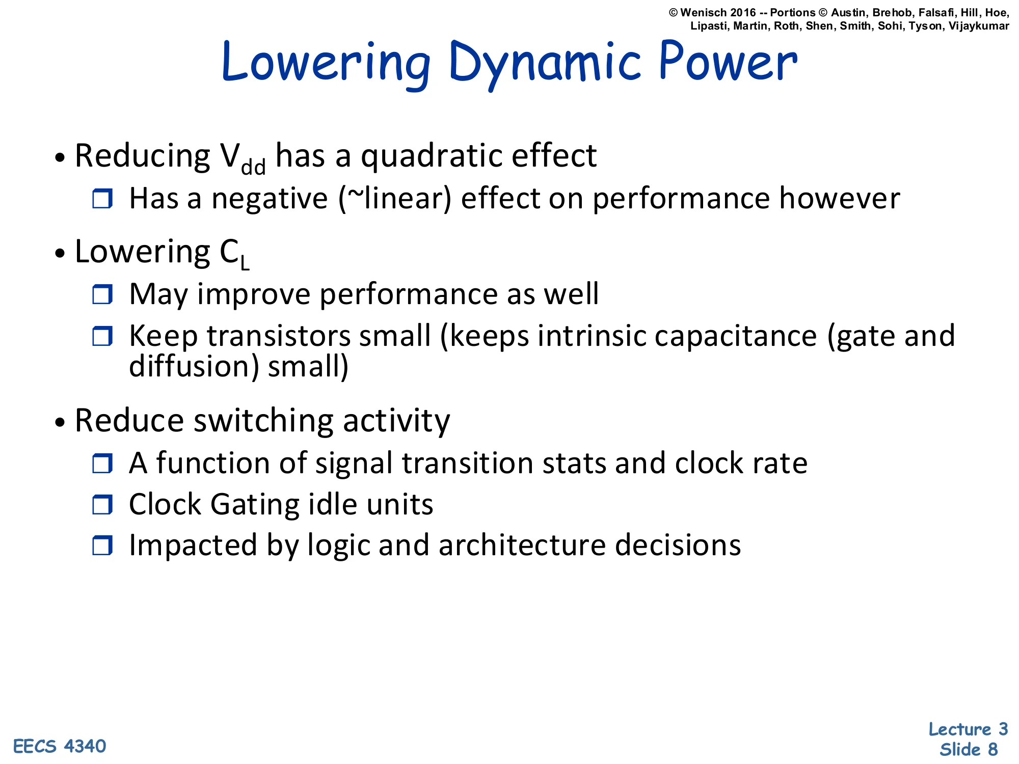
Lowering Dynamic Power
- Reducing Vdd has a quadratic effect
- Has a negative (~linear) effect on performance however
- Lowering CL
- May improve performance as well
- Keep transistors small (keeps intrinsic capacitance (gate and diffusion) small)
- Reduce switching activity
- A function of signal transition stats and clock rate
- Clock Gating idle units
- Impacted by logic and architecture decisions
Each lever in 21CV2Af has a different cost-benefit profile. Voltage is the most powerful lever — quadratic in power — but it is approximately linear in delay, so dropping Vdd slows the part by roughly the same factor that it shrinks V. That asymmetry is exactly why dynamic voltage/frequency scaling is attractive: a small voltage cut buys a big power cut for a modest performance hit. Lowering load capacitance CL — through smaller transistors, shorter wires, low-k dielectrics — is purely beneficial because smaller capacitors charge faster, so f can rise. Activity factor is the architect’s playground: clock gating disables the clock to idle functional units so their flip-flops don’t toggle on every cycle, and broader logic-level decisions (e.g., bus encoding, operand isolation, narrow-width detection) all reduce A. Together these techniques are what let real chips stay below their power budget despite each generation’s transistor budget growing.
DVFS: Dynamic Voltage/Frequency Scaling
Show slide text
DVFS: Dynamic Voltage/Frequency Scaling
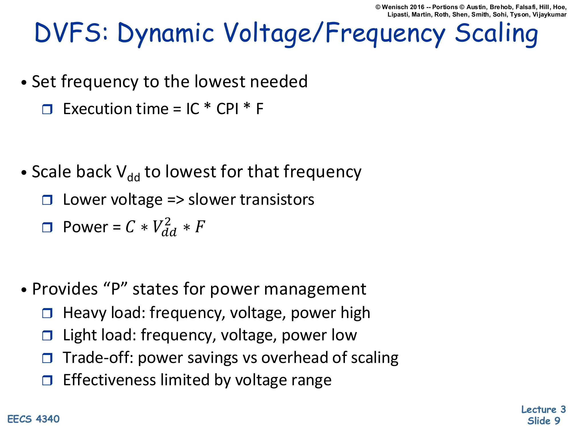
- Set frequency to the lowest needed
- Execution time = IC * CPI * F
- Scale back Vdd to lowest for that frequency
- Lower voltage => slower transistors
- Power=C∗Vdd2∗F
- Provides “P” states for power management
- Heavy load: frequency, voltage, power high
- Light load: frequency, voltage, power low
- Trade-off: power savings vs overhead of scaling
- Effectiveness limited by voltage range
DVFS exploits the asymmetric voltage-vs-delay relationship from the previous slide. The chip detects how much performance the current workload actually demands, then drops f to the slowest setting that still meets that demand and drops Vdd to the lowest level that still keeps the transistors fast enough to run at that f. Because P∝CV2f and V tracks f roughly linearly, the operating point near peak frequency burns power roughly cubically: a small frequency cut yields an outsized power cut. ACPI exposes these operating points as “P-states” (P0, P1, P2, …), and the OS or firmware picks among them based on utilization. The slide flags two real limits: switching between P-states has latency (the PLL must relock, the regulator must settle), so blindly toggling on every short idle costs more than it saves; and at the low end the voltage cannot go below the SRAM/flop minimum-retention voltage, which caps how deeply DVFS can scale before more aggressive techniques (power gating entire blocks) are required.
Combined Power-Performance Metrics
Show slide text
Combined Power-Performance Metrics
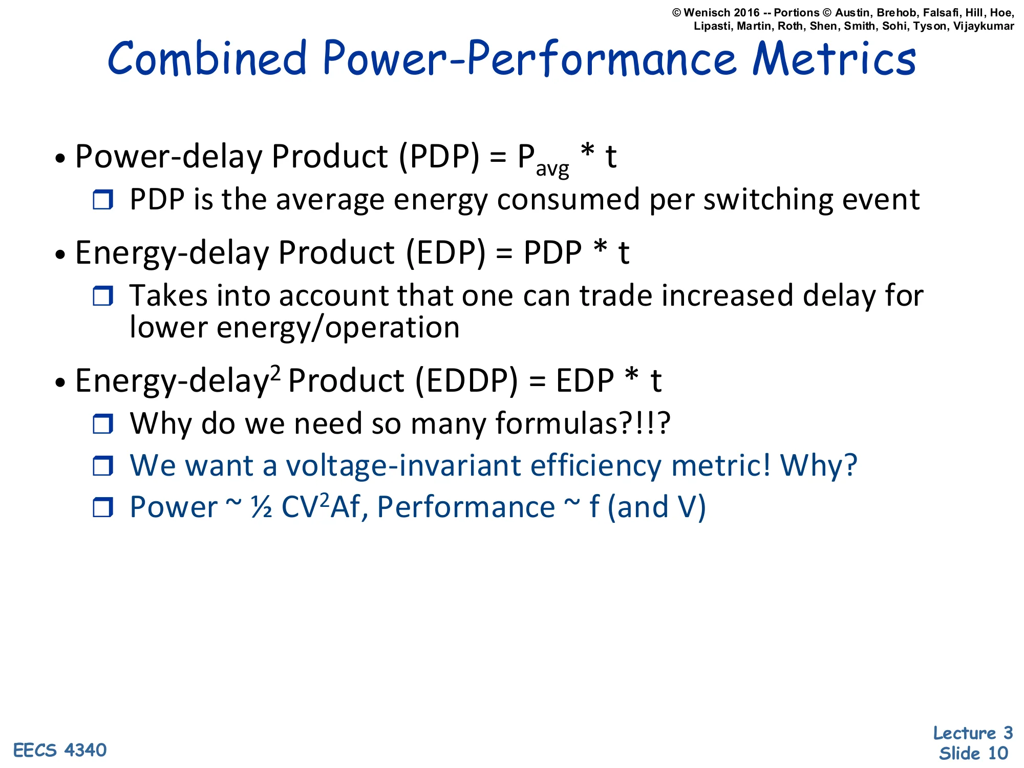
- Power-delay Product (PDP) = Pavg⋅t
- PDP is the average energy consumed per switching event
- Energy-delay Product (EDP) = PDP ⋅ t
- Takes into account that one can trade increased delay for lower energy/operation
- Energy-delay2 Product (EDDP) = EDP ⋅ t
- Why do we need so many formulas?!?
- We want a voltage-invariant efficiency metric! Why?
- Power ∼21CV2Af, Performance ∼f (and V)
Energy alone (PDP) is misleading because you can always make a chip use less energy per task by running it slower — which is rarely what users want. Multiplying by delay t once gives EDP, which penalizes slow designs symmetrically with energy-hungry ones, so a 2× faster design and a 2× more energy-efficient design score the same. Multiplying by delay twice gives ED²P, which leans further toward speed: the same trade can be lost on ED²P even when EDP improves, as the next slide shows. The slide’s deeper point is that V scales both numerator and denominator of these metrics: power has V2, performance scales roughly with V. ED²P happens to be voltage-invariant — if you adjust V alone, both factors track and the metric stays constant. That property makes ED²P the right metric for comparing two microarchitectures independent of where each one happens to be tuned on its DVFS curve.
E vs. EDP vs. ED²P (Worked Example)
Show slide text
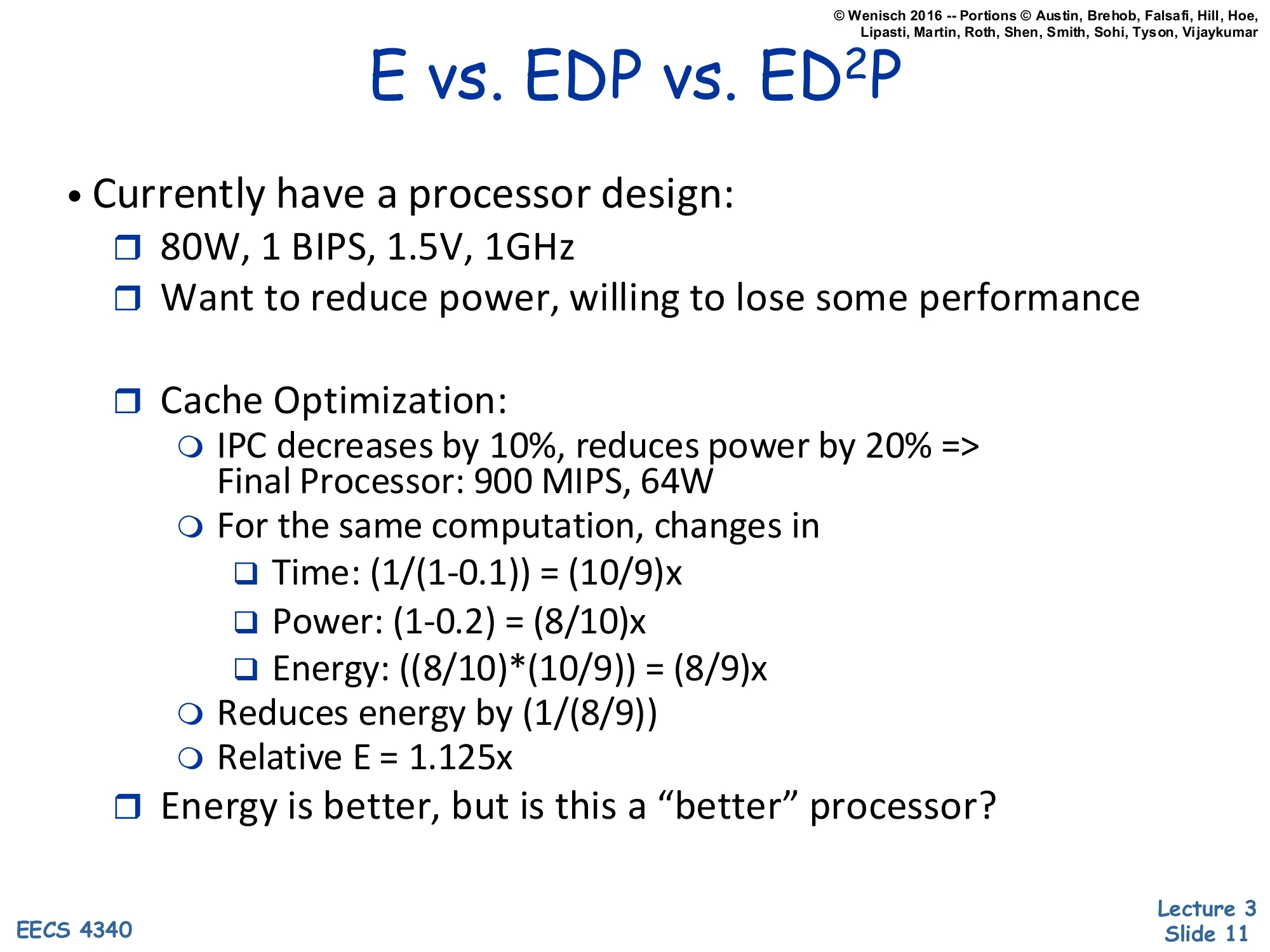
E vs. EDP vs. ED²P
- Currently have a processor design:
- 80W, 1 BIPS, 1.5V, 1GHz
- Want to reduce power, willing to lose some performance
- Cache Optimization:
- IPC decreases by 10%, reduces power by 20% => Final Processor: 900 MIPS, 64W
- For the same computation, changes in
- Time: (1/(1−0.1))=(10/9)x
- Power: (1−0.2)=(8/10)x
- Energy: ((8/10)∗(10/9))=(8/9)x
- Reduces energy by (1/(8/9))
- Relative E = 1.125x
- Energy is better, but is this a “better” processor?
The example walks through the arithmetic carefully. A cache change cuts IPC by 10% (so the same program now takes 1/0.9=10/9 as long) but saves 20% of power (so power scales by 8/10). Energy is power × time, (8/10)(10/9)=8/9, meaning the same workload finishes consuming 98 of its previous energy — about 12.5% less. Phrased the other way, the relative energy of the new design is 1/(8/9)=9/8=1.125× better than baseline. So strictly on energy, the optimization wins. But the iron law warns that throughput dropped: the new chip runs at 900 MIPS instead of 1000 MIPS, and the user feels that. The slide ends with the deliberately provocative question — is this really a better processor? — which the next slide answers in the negative once we score the same change with EDP and ED²P.
Not necessarily — comparing to DVFS
Show slide text
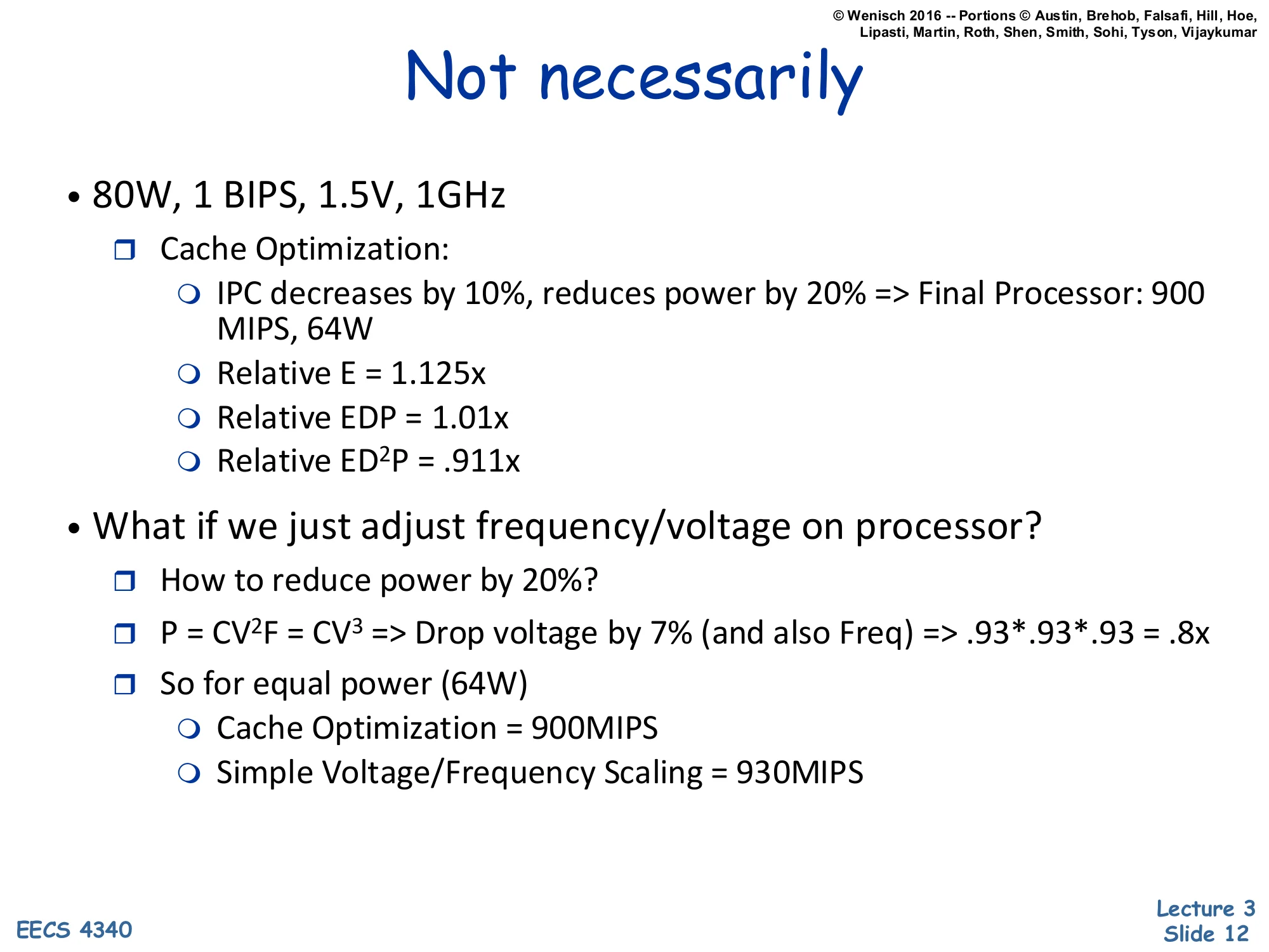
Not necessarily
- 80W, 1 BIPS, 1.5V, 1GHz
- Cache Optimization:
- IPC decreases by 10%, reduces power by 20% => Final Processor: 900 MIPS, 64W
- Relative E = 1.125x
- Relative EDP = 1.01x
- Relative ED²P = .911x
- Cache Optimization:
- What if we just adjust frequency/voltage on processor?
- How to reduce power by 20%?
- P=CV2F=CV3 => Drop voltage by 7% (and also Freq) => 0.93×0.93×0.93=0.8x
- So for equal power (64W)
- Cache Optimization = 900 MIPS
- Simple Voltage/Frequency Scaling = 930 MIPS
Continuing from slide 11: the relative EDP for the cache change is 1.125×(10/9)≈1.01× — virtually break-even — and ED²P actually drops to 0.911×, meaning the new design loses on the voltage-invariant efficiency metric. The slide then asks what would happen if we simply ran DVFS on the original design to hit the same 64W power budget. With P∝V2f and V∝f (in the linear-delay regime), P∝V3, so a 7% voltage cut yields 0.933≈0.8× power — the desired 20% reduction. At that operating point the original processor delivers 930 MIPS, which is better than the cache-optimized 900 MIPS at the same 64W. This is the canonical result that motivates ED²P: cache optimization looked great on energy but lost to plain DVFS on actual performance-per-watt, so the cache change is only worthwhile if it stacks with DVFS, not as a substitute for it.
Class Problem (If Time)
Show slide text
Class Problem (If Time)
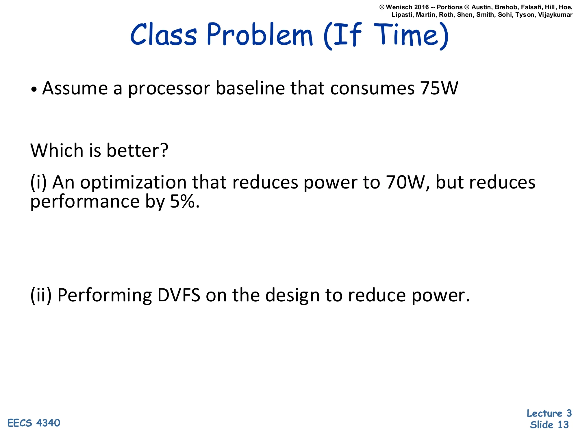
- Assume a processor baseline that consumes 75W
Which is better?
(i) An optimization that reduces power to 70W, but reduces performance by 5%.
(ii) Performing DVFS on the design to reduce power.
Practice problem: compare a fixed microarchitectural optimization against DVFS on the unmodified baseline. Both options aim to lower power; the question is which gives a better operating point. Option (i) cuts power from 75W to 70W (a 6.7% reduction) but at the cost of a 5% performance drop. Option (ii) leaves the design alone but uses voltage/frequency scaling to whatever power level matches a 5% performance drop, then we compare the resulting power. Because P∝V3 when V∝f, even a small frequency cut buys a much larger power cut, so DVFS is expected to win. The next slide works out the algebra.
Class Problem — Solution
Show slide text
Class Problem (If Time) — Solution
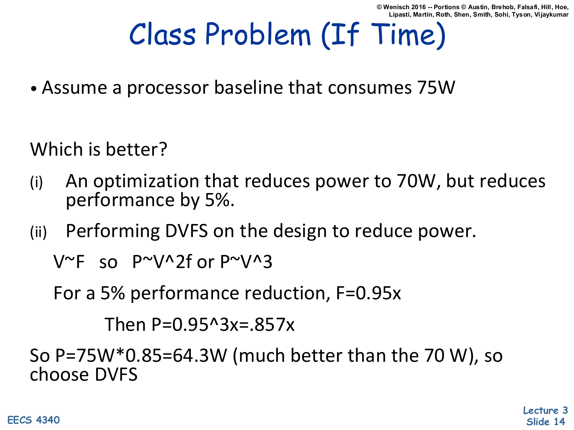
Assume a processor baseline that consumes 75W
(i) An optimization that reduces power to 70W, but reduces performance by 5%.
(ii) Performing DVFS on the design to reduce power.
V∼F so P∼V2f or P∼V3
For a 5% performance reduction, F=0.95x
Then P=0.953x=0.857x
So P=75W⋅0.85=64.3W (much better than the 70W), so choose DVFS.
The arithmetic confirms the intuition. If we accept the same 5% performance reduction via DVFS, frequency drops to 0.95×. With V∝f in the dynamic-voltage regime, voltage also scales by 0.95, and dynamic power scales by V2f=0.953≈0.857. Applied to the 75W baseline, that is ≈64.3W — substantially below the 70W achieved by option (i). DVFS wins because it captures the cubic-in-voltage scaling that any architectural trick is competing against. The lesson generalizes: for any candidate optimization that costs performance, ask whether DVFS would do better at the same performance budget; if not, the optimization is only useful as a stacking technique on top of DVFS, not in place of it.
The Execution Core: Pipelining
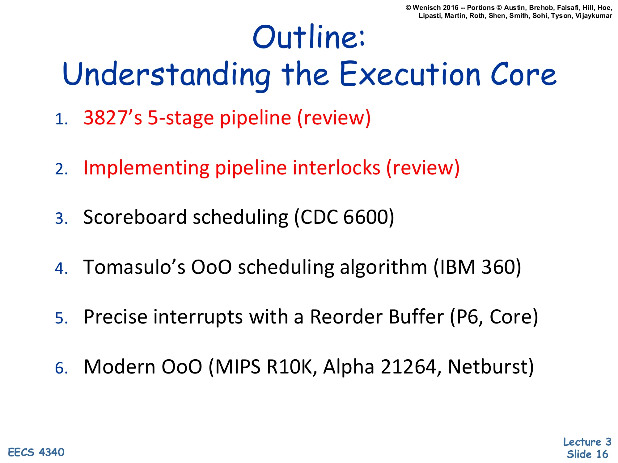
Outline: Understanding the Execution Core
Show slide text
Outline: Understanding the Execution Core
- 3827’s 5-stage pipeline (review)
- Implementing pipeline interlocks (review)
- Scoreboard scheduling (CDC 6600)
- Tomasulo’s OoO scheduling algorithm (IBM 360)
- Precise interrupts with a Reorder Buffer (P6, Core)
- Modern OoO (MIPS R10K, Alpha 21264, Netburst)
This roadmap orders execution-core ideas by historical and conceptual progression. Steps 1–2 (the focus of L03) are the in-order, statically scheduled 5-stage pipeline borrowed from EECS 3827, plus the interlock logic that stalls the pipe when dependencies aren’t ready. Step 3 (scoreboarding from CDC 6600, 1964) is the first hardware scheme that issues instructions out of order without renaming. Step 4 (Tomasulo’s algorithm from the IBM 360/91, 1967) added reservation stations, the common data bus, and implicit register renaming, making it the foundation of every modern OoO core. Step 5 introduces the reorder buffer used in Intel’s P6 family to deliver precise interrupts on top of speculative execution. Step 6 lists the canonical modern OoO designs that combine all of the above plus aggressive branch prediction and large physical register files. The note “3827” refers to a Columbia logic-design course; the deployed site is EECS 4340.
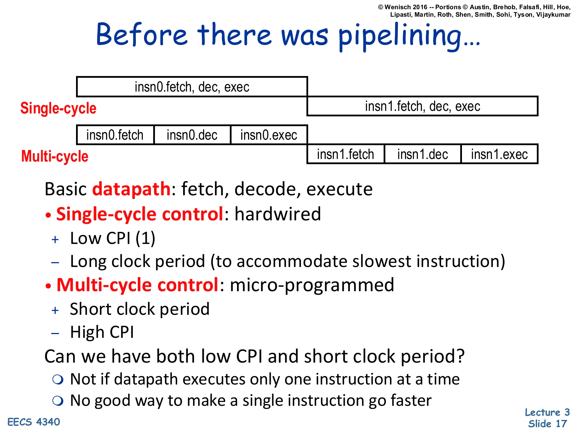
Before there was pipelining…
Show slide text
Before there was pipelining…
Single-cycle vs. Multi-cycle datapath timeline:
- Single-cycle: insn0.fetch, dec, exec then insn1.fetch, dec, exec — one long box per instruction.
- Multi-cycle: insn0.fetch | insn0.dec | insn0.exec then insn1.fetch | insn1.dec | insn1.exec — three short boxes per instruction.
Basic datapath: fetch, decode, execute
Single-cycle control: hardwired
- Low CPI (1) – Long clock period (to accommodate slowest instruction)
Multi-cycle control: micro-programmed
- Short clock period – High CPI
Can we have both low CPI and short clock period?
- Not if datapath executes only one instruction at a time
- No good way to make a single instruction go faster
This is the motivating contrast. A single-cycle datapath uses one wide combinational path that completes fetch, decode, and execute in one long clock period; the CPI is exactly 1 but the cycle time is set by the slowest instruction (typically a load, which must wait for memory). A multi-cycle datapath chops the work into small steps (fetch, decode, execute) executed in successive cycles, so each step’s clock can be short, but each instruction now needs multiple cycles, inflating CPI. Both designs share a fundamental limitation: they execute exactly one instruction at a time, so improving program time means making that one instruction faster — and there is no good way to do that once you’ve reached the limits of the technology. Pipelining breaks the tie by overlapping the execution of multiple instructions: short cycle (like multi-cycle) and ~1 CPI (like single-cycle), at the cost of new hardware to hold per-stage state and resolve hazards.
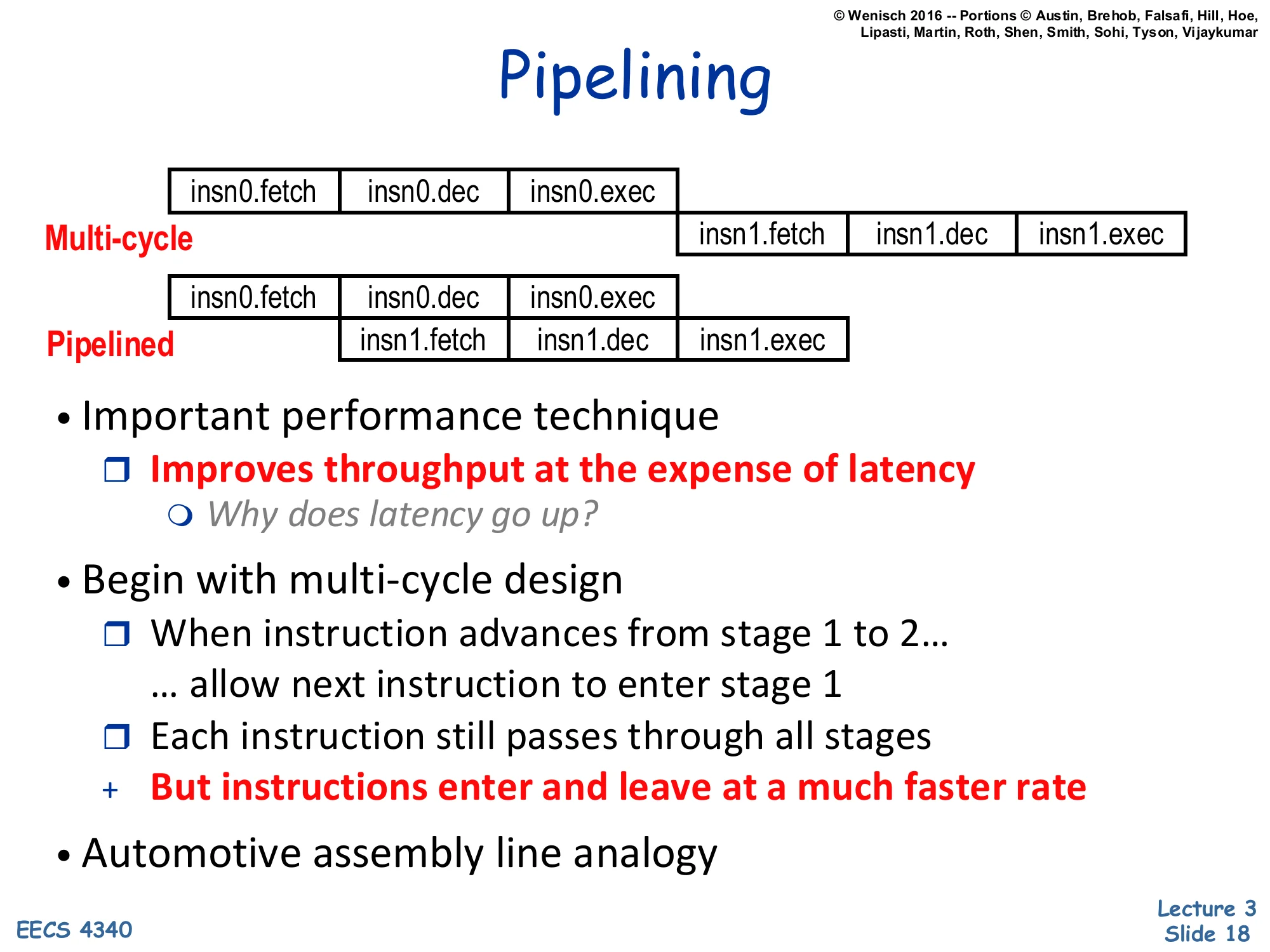
Pipelining
Show slide text
Pipelining
Multi-cycle: insn0.fetch | insn0.dec | insn0.exec → then insn1.fetch | insn1.dec | insn1.exec
Pipelined: insn0.fetch | insn0.dec | insn0.exec — and one cycle later insn1.fetch | insn1.dec | insn1.exec runs concurrently in earlier stages.
- Important performance technique
- Improves throughput at the expense of latency
- Why does latency go up?
- Improves throughput at the expense of latency
- Begin with multi-cycle design
- When instruction advances from stage 1 to 2… … allow next instruction to enter stage 1
- Each instruction still passes through all stages
- But instructions enter and leave at a much faster rate
- Automotive assembly line analogy
Pipelining is the key insight: once instruction i moves out of stage 1, the stage-1 hardware is idle and can immediately start fetching instruction i+1. Steady-state throughput rises from one instruction per several cycles to one instruction per cycle. The cost is latency per instruction: each instruction now incurs the propagation delay of every pipeline register on its way through the pipe, so any single instruction takes slightly longer than it would in a multi-cycle design. The slide flags this trade-off in red: throughput improves at the expense of latency, which is why pipelining is justified for throughput-bound workloads but doesn’t help a single critical-path instruction. The factory analogy is a literal one: an automotive assembly line lets many cars be in different stages of assembly simultaneously, dramatically increasing cars-per-hour even though each individual car still takes the same total time to build.
Pipeline Illustrated: Bandwidth scales with depth
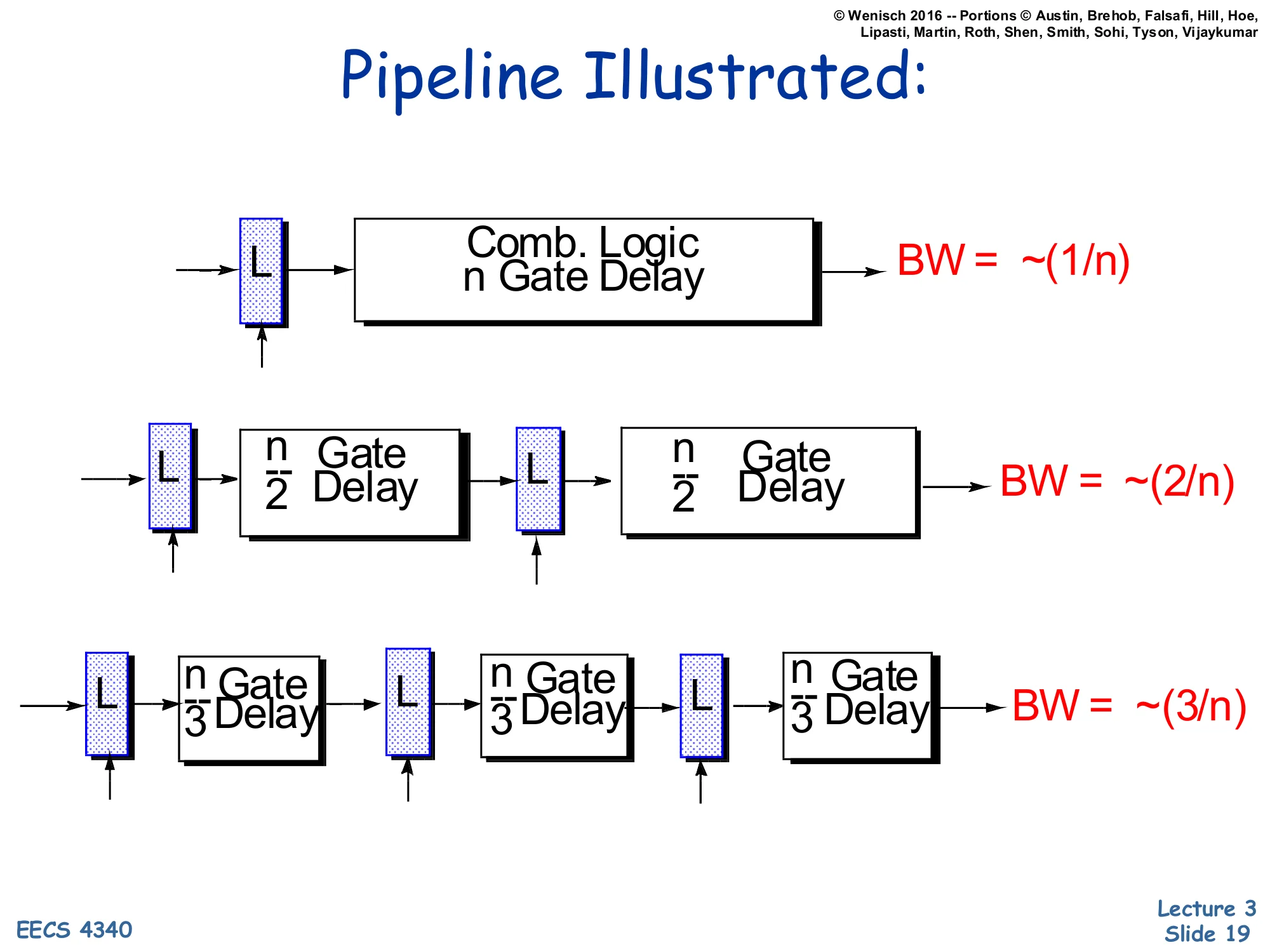
Show slide text
Pipeline Illustrated
- Top row: latch (L) → Combinational logic, n Gate Delay → BW = ∼(1/n)
- Middle row: L→n/2 delay →L→n/2 delay → BW = ∼(2/n)
- Bottom row: L→n/3→L→n/3→L→n/3 → BW = ∼(3/n)
The diagram quantifies why pipelining works. With one combinational block of total delay n gates, the bandwidth (instructions per gate-time) is ∼1/n because each new operation must wait for the entire n gates to finish. Splitting that block in half with a latch in the middle lets two operations be in flight: while the first half-result is latched and re-evaluated by the second half, a new input enters the first half. The clock period is now set by the longer half (n/2), so bandwidth doubles to ∼2/n. Splitting into three balanced stages triples bandwidth to ∼3/n, and so on. In an idealized world this scales without limit, but real pipelines hit two ceilings: the latch insertion overhead (setup, hold, clock-to-Q) becomes a non-trivial fraction of the smaller stage delays, and stage imbalance means the slowest stage caps the achievable f. That is why pipeline depth is bounded in practice — see slide 45’s Pentium 4 cautionary note.
3827 Processor Pipeline Review
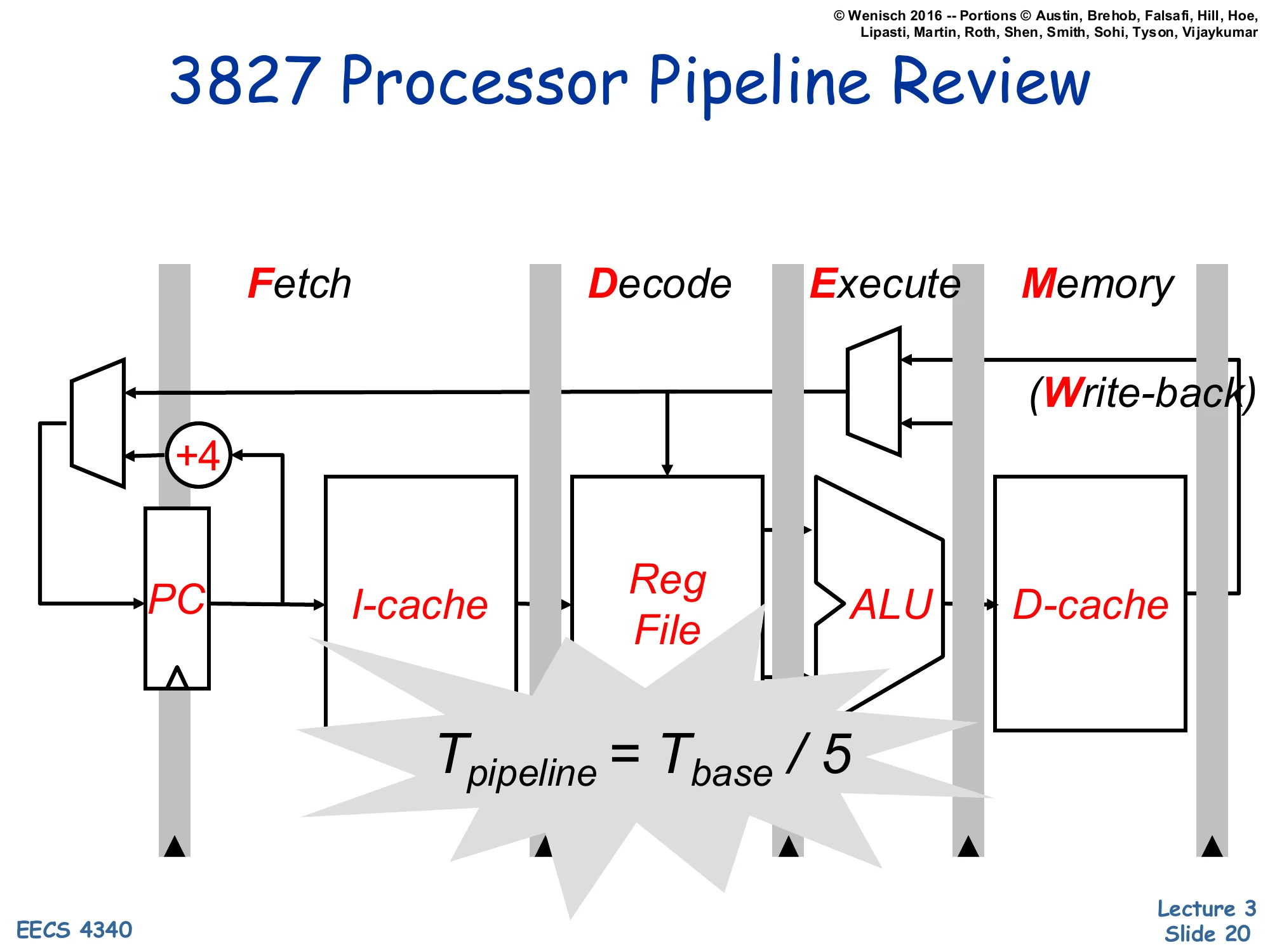
Show slide text
3827 Processor Pipeline Review
Five stages: Fetch | Decode | Execute | Memory | Write-back
Blocks per stage:
- Fetch: PC, +4, I-cache
- Decode: Reg File
- Execute: ALU
- Memory: D-cache
- Write-back: write port back to Reg File
Tpipeline=Tbase/5
This is the canonical 5-stage RISC pipeline from EECS 4340’s prerequisite logic-design course (referred to here as 3827). Fetch reads the next instruction from the I-cache and increments the PC. Decode reads the source registers from the register file and prepares control signals. Execute runs the ALU (or computes a memory address, or evaluates a branch condition). Memory accesses the D-cache for loads and stores. Write-back writes the result into the destination register. Under ideal conditions — balanced stage delays and no hazards — clock period is one-fifth of the unpipelined cycle, giving 5× throughput. The next several slides walk through each stage individually and the pipeline registers between them (IF/ID, ID/EX, EX/Mem, Mem/WB) that hold per-instruction state from one cycle to the next.
Stage 1: Fetch
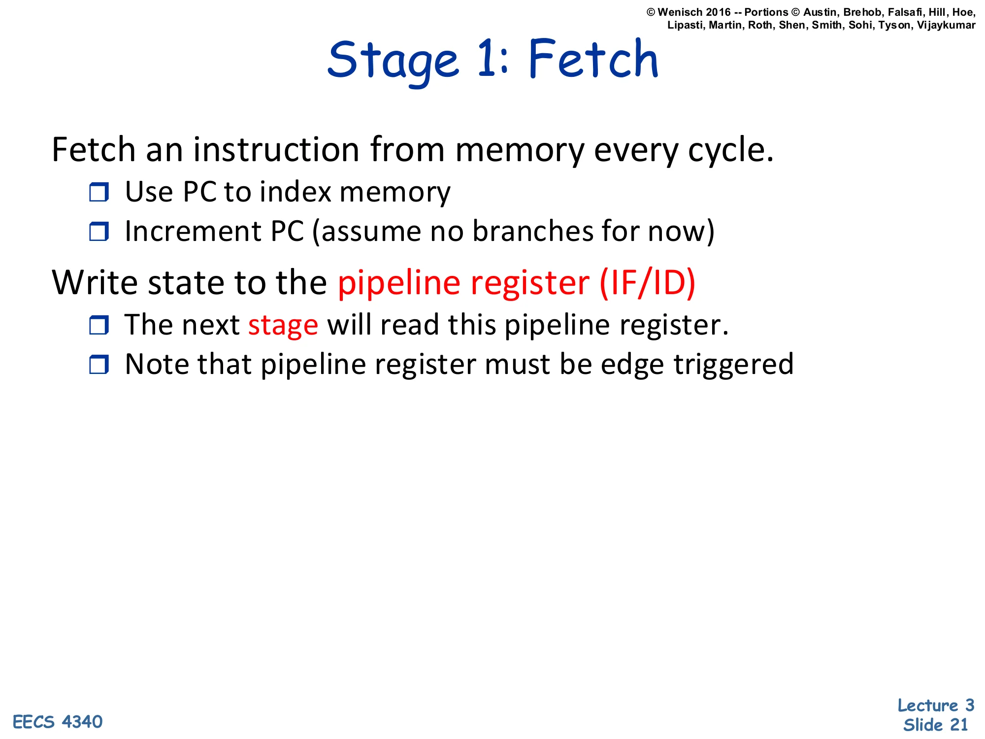
Show slide text
Stage 1: Fetch
Fetch an instruction from memory every cycle.
- Use PC to index memory
- Increment PC (assume no branches for now)
Write state to the pipeline register (IF/ID)
- The next stage will read this pipeline register.
- Note that pipeline register must be edge triggered
Fetch is the simplest stage. The PC indexes the I-cache, the returned instruction bits are written to the IF/ID pipeline register, and the PC is incremented in parallel by an adder hard-wired to +1 (one instruction-word; in MIPS that would be +4 bytes). The slide’s emphasis on the pipeline register being edge triggered matters because each stage must observe a stable input for an entire cycle — a level-sensitive latch would let Stage 2 see Stage 1’s mid-cycle transients. Branch handling is deferred to L04 (this lecture assumes straight-line code): once branches enter the picture, fetch must speculate on the next-PC value, which is what motivates branch prediction later in the course. The simplifying assumption “no branches” means PC always becomes PC+1 next cycle, which is why the diagram on the next slide shows only a +1 adder feeding back through a MUX.
Fetch datapath
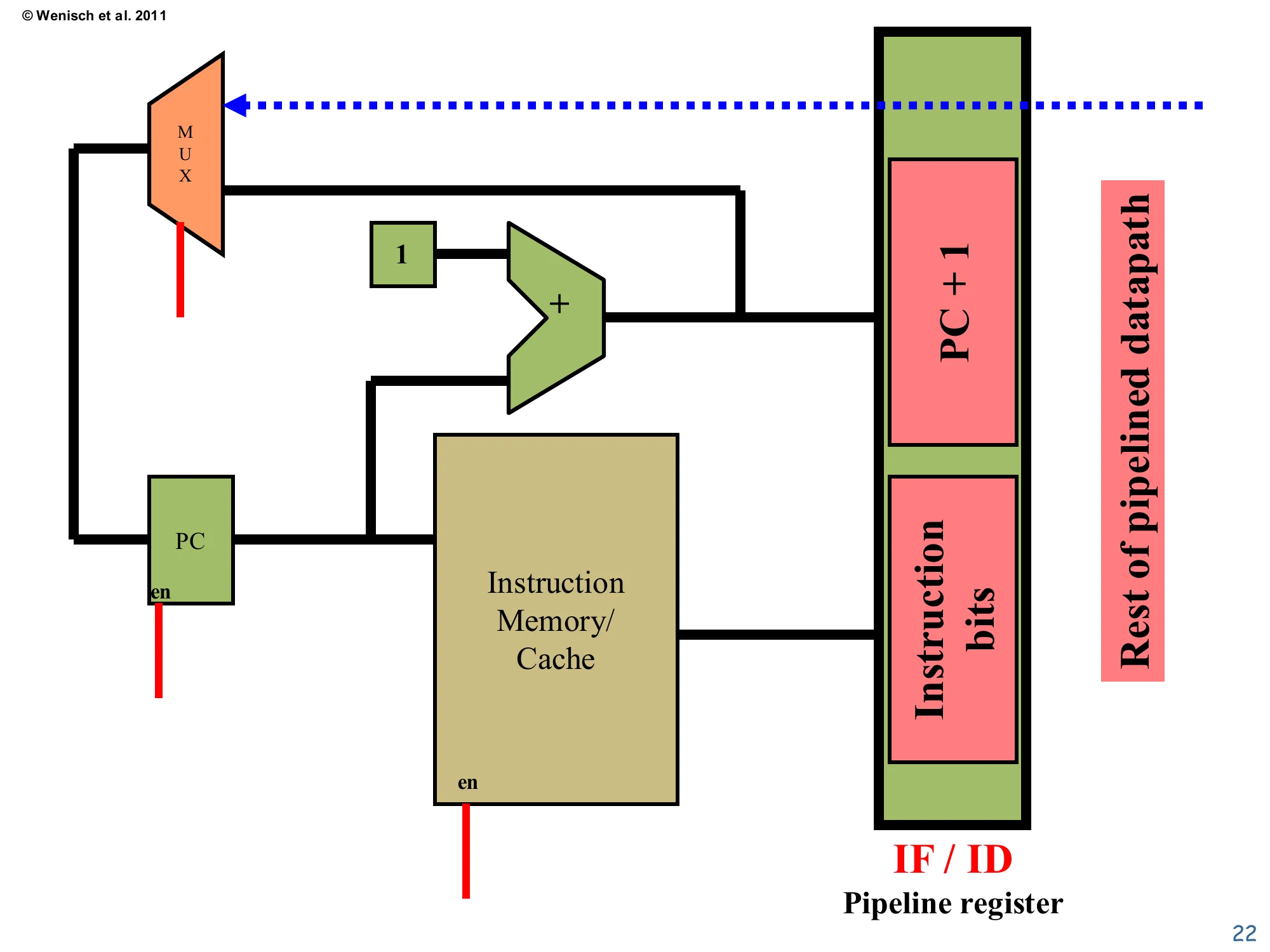
Show slide text
Fetch datapath
MUX → PC (en) → Instruction Memory/Cache → IF/ID pipeline register fields: PC + 1, Instruction bits.
The MUX selects between PC+1 (the +1 adder output, with constant 1) and a feedback path (dotted) that will later carry branch targets from a deeper pipeline stage.
The schematic shows the physical implementation of stage 1. The PC register feeds two consumers: the instruction memory/cache (which returns the encoded instruction word) and a +1 adder (which produces the sequential next-PC). A MUX in front of the PC chooses between sequential next-PC and an alternative source — the dotted line shows where a branch target will eventually come back from the Execute stage to override sequential fetch. Both the PC register and the I-cache have an en input; the I-cache en enables the read and the PC en allows the register to update. These enables are critical when stalls are introduced: deasserting them freezes the front end while later stages catch up. The IF/ID pipeline register on the right captures both the fetched instruction bits and PC+1 (which downstream stages will need for branch-target computation and PC-relative arithmetic).
Stage 2: Decode
Show slide text
Stage 2: Decode
Decodes opcode bits
- May set up control signals for later stages
Read input operands from registers file
- specified by regA and regB of instruction bits
Write state to the pipeline register (ID/EX)
- Opcode
- Register contents
- Offset & destination fields
- PC+1 (even though decode didn’t use it)
Decode does two parallel jobs. First, it interprets the opcode bits to generate the control signals that downstream stages will need (ALU operation code, mem-read/write, register-write enable, MUX selects). Second, it reads up to two source registers from the register file, indexed by the regA and regB fields of the encoded instruction. Both pieces of information are bundled into the ID/EX pipeline register so that Execute can act on them next cycle. The slide emphasizes that PC+1 is also propagated forward even though Decode itself doesn’t use it — branch instructions in Execute will need PC+1+offset to compute their target, and storing PC+1 here saves having to redo the +1 adder later. The register file in this 5-stage design is read in Decode and written in Write-back, which means a write to a register and a read of the same register on the same cycle requires either a half-cycle write/read split or explicit forwarding (covered in L04).
Decode datapath
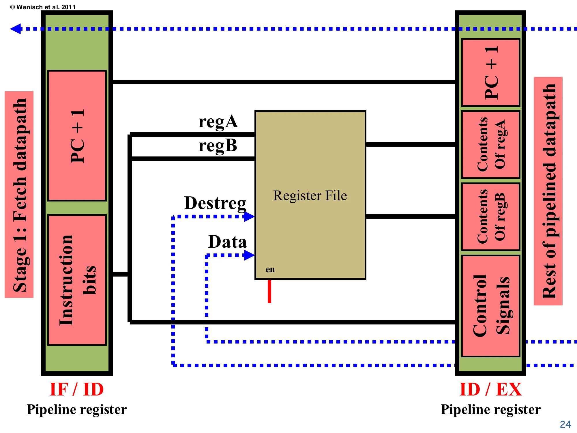
Show slide text
Decode datapath
IF/ID carries: PC+1, Instruction bits.
The regA and regB fields select reads from the Register File. The Destreg and Data inputs (dotted, fed from a later stage) implement write-back. The ID/EX pipeline register captures: PC+1, Contents of regA, Contents of regB, and Control Signals.
The schematic shows the register file with two read ports (output regA and regB contents) and one write port (Destreg index plus Data — both arrive on dotted lines from the Mem/WB stage). The regA and regB indexes come straight from instruction-bit fields so that decode happens in parallel with the read. The control signals box on the bottom right of ID/EX is the bundle of MUX selects, ALU op code, and enable signals that decode produces from the opcode; later stages just consume those signals without re-examining the opcode. The ID/EX register’s PC+1 field is the same value forwarded from IF/ID, kept alive for the branch adder in Execute. This stage’s critical timing assumption is that the register-file read completes in a single cycle along with the opcode decode — for a small register file in a 5-stage RISC design this is comfortable, but in higher-frequency designs the read can itself take multiple cycles and the pipeline grows accordingly.
Stage 3: Execute
Show slide text
Stage 3: Execute
Perform ALU operation.
- Input operands can be:
- Contents of regA or RegB
- Offset field on the instruction
- Branches: calculate PC+1+offset
Write state to the pipeline register (EX/Mem)
- ALU result, contents of RegB and PC+1+offset
- Instruction bits for opcode and destReg specifiers
Execute is where the actual computation happens. The ALU’s two inputs come from a MUX: one input is regA, the other is either regB (for register-register operations like add) or the sign-extended offset field (for immediate forms and address calculation). For branches and PC-relative jumps, a separate adder computes PC+1+offset as the candidate target. The EX/Mem pipeline register carries forward four things: the ALU result (which is either the arithmetic answer or a memory address), the contents of regB (needed in case this is a store, where regB is the data to write), the branch target, and the destReg specifier plus opcode (so that Memory and Write-back know what to do). This is the stage where the design’s arithmetic critical path lives — the ALU’s gate delay typically caps the achievable clock frequency in a balanced 5-stage pipeline.
Execute datapath
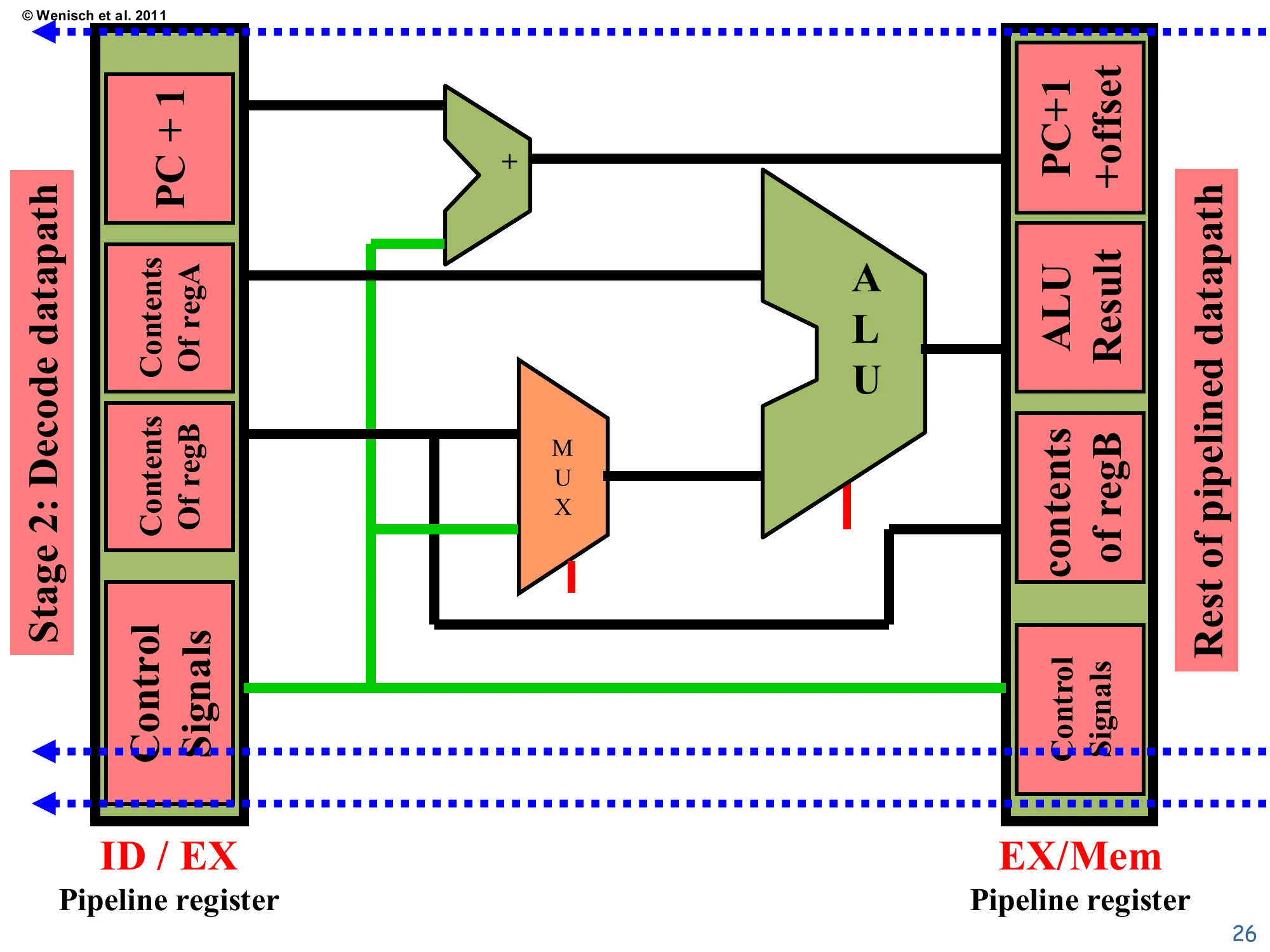
Show slide text
Execute datapath
From ID/EX: PC+1, Contents of regA, Contents of regB, offset, Control Signals.
A + adder computes PC+1+offset → target. The ALU takes regA on one side and (regB or offset) selected by a MUX on the other. The EX/Mem pipeline register captures: PC+1+offset, ALU result, contents of regB, Control Signals.
The schematic shows the two adders that live in Execute: the dedicated branch adder on top (PC+1 plus the sign-extended offset, producing the branch target) and the main ALU on the bottom. The MUX feeding the ALU’s second input is controlled by the decode-time control signals — for an add it routes regB, for an immediate-form addi or for a load/store address calculation it routes the offset. The contents of regB are also propagated forward (green wire) to the EX/Mem register because stores need that value during Memory; arithmetic instructions ignore it. Notice that the destReg specifier and opcode (control signals) flow straight through Execute without modification — Execute only cares about what to compute, not where to store the result. This separation of concerns is exactly what makes the pipeline modular: each stage touches just the fields it needs and forwards the rest unchanged.
Stage 4: Memory Operation
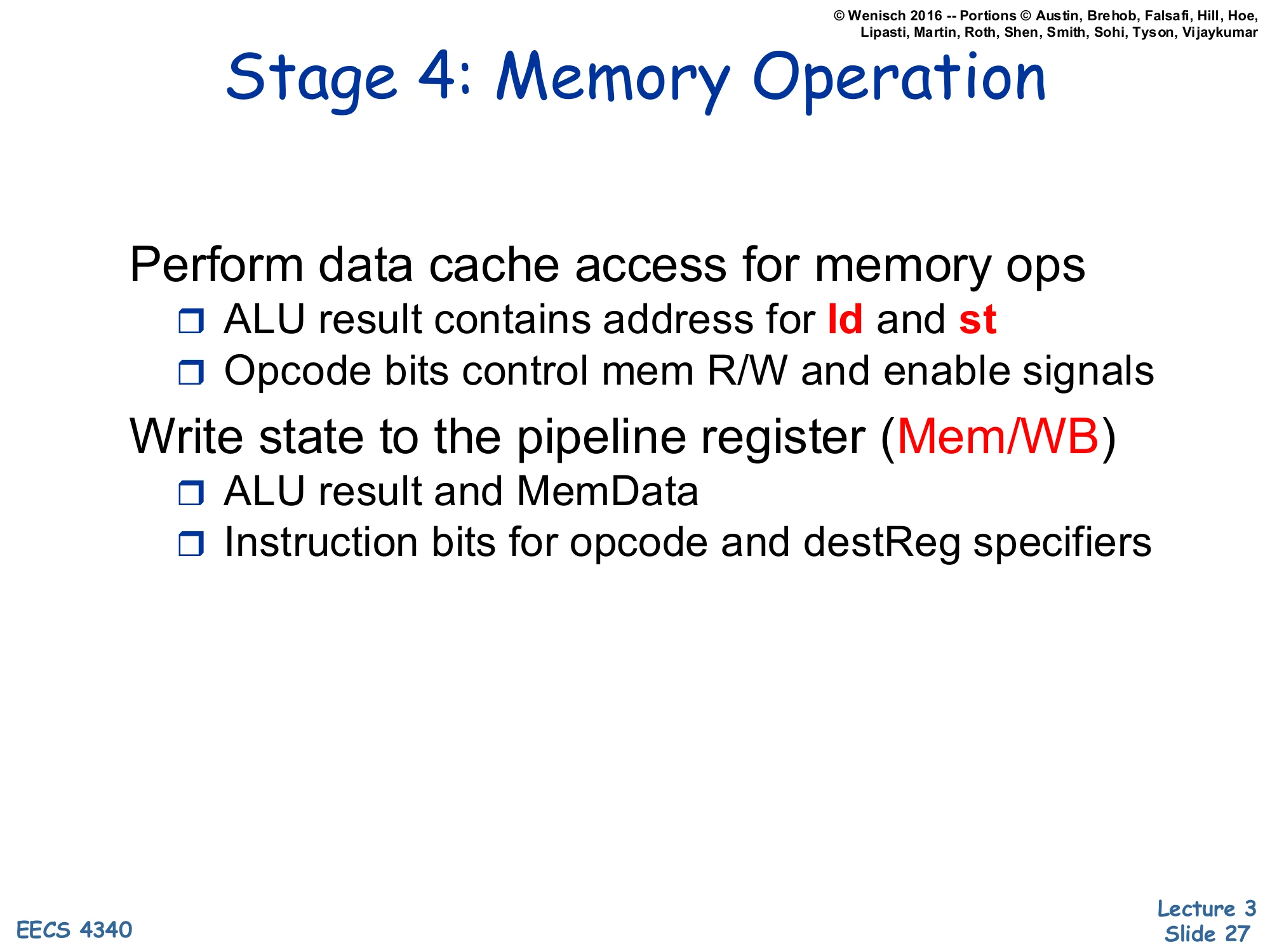
Show slide text
Stage 4: Memory Operation
Perform data cache access for memory ops
- ALU result contains address for ld and st
- Opcode bits control mem R/W and enable signals
Write state to the pipeline register (Mem/WB)
- ALU result and MemData
- Instruction bits for opcode and destReg specifiers
Stage 4 services memory operations. For a load (ld), the D-cache is read using the ALU-computed address and the returned data is written to the Mem/WB pipeline register as MemData; the ALU result is passed through unused. For a store (st), the regB value carried forward from Execute is written to the D-cache at the ALU-computed address — there is no result to forward to Write-back. For arithmetic and logical instructions, the D-cache is disabled (read=0, write=0) and the ALU result is simply forwarded through Mem/WB so Write-back can put it in the register file next cycle. The opcode bits, threaded all the way down from Decode through the pipeline registers, gate the cache R/W and enable signals. This stage’s latency is what motivates the Memory stage’s existence at all — if memory always answered in zero time, Memory and Execute could be merged. In real chips, even an L1 D-cache hit takes 2–4 cycles, which becomes a key driver of deeper pipelines later in the course.
Memory datapath
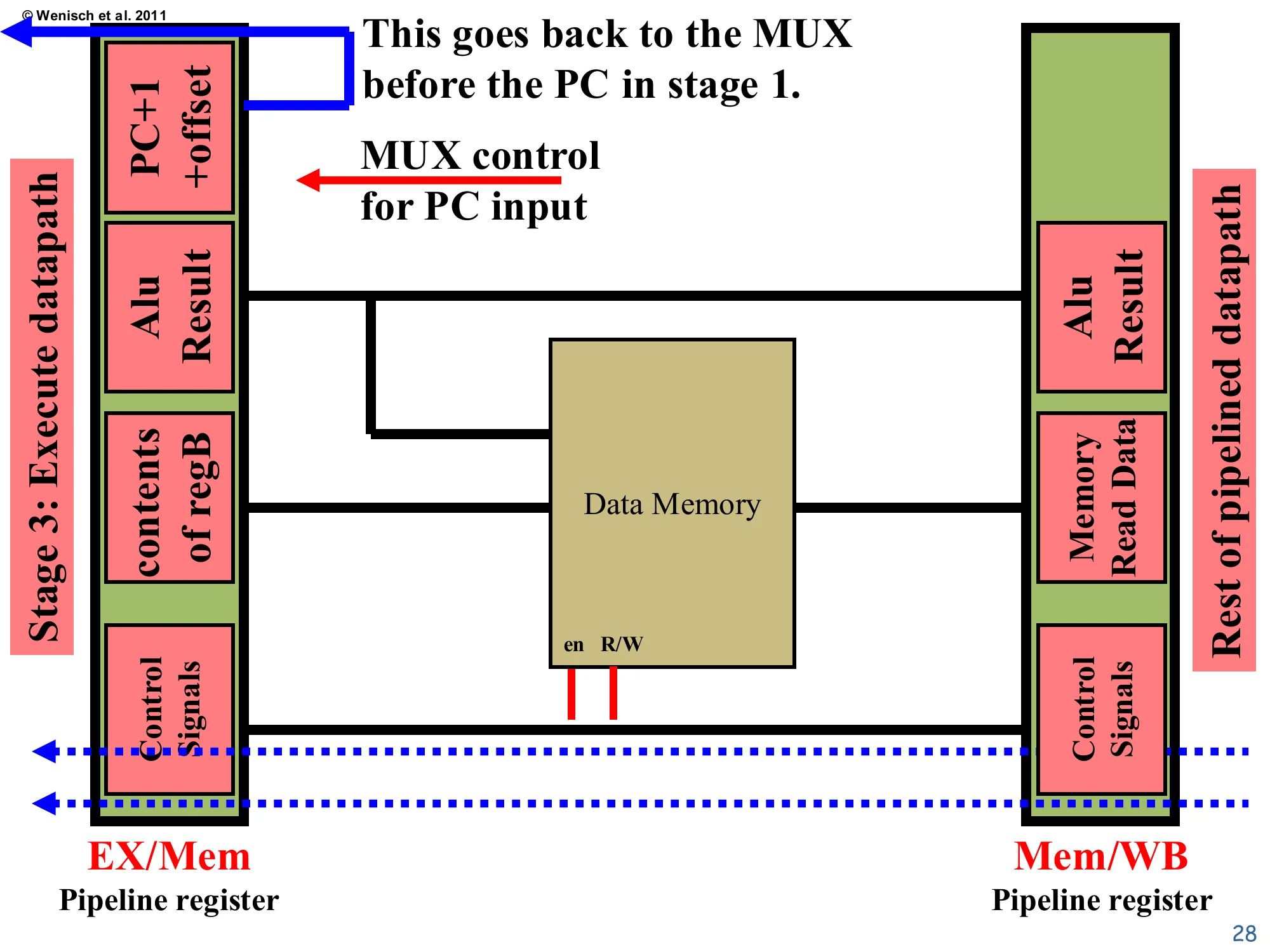
Show slide text
Memory datapath
From EX/Mem: PC+1+offset, ALU result, contents of regB, Control Signals.
The Data Memory has en and R/W enables driven by control signals. ALU result drives the address; contents of regB drive write-data; the read port produces Memory Read Data into the Mem/WB pipeline register, alongside ALU result and Control Signals.
Note: PC+1+offset (target) feeds back to the MUX before the PC in stage 1 — this is the branch redirect path.
The Memory schematic mirrors the description on the previous slide. The ALU result wire becomes the address line into Data Memory, regB becomes the write data, and the read port output is captured into Mem/WB as Memory Read Data. The en and R/W signals on the bottom are gated by the opcode-derived control bits — a load asserts en=1, R/W=read; a store asserts en=1, R/W=write; arithmetic instructions deassert en. The annotation at the top — “This goes back to the MUX before the PC in stage 1” — is critical: this is how branch targets and jumps redirect fetch. In this lecture’s idealized pipeline, the redirect happens in Memory, which means a taken branch wastes three fetched instructions (those in IF, ID, EX behind the branch) — that bubble is the control hazard analyzed quantitatively in L04.
Stage 5: Write back
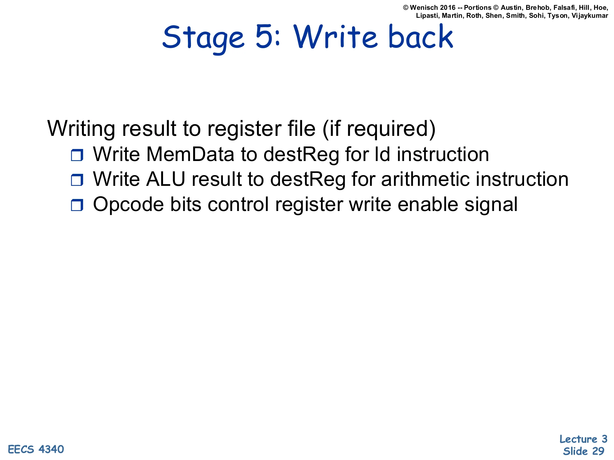
Show slide text
Stage 5: Write back
Writing result to register file (if required)
- Write MemData to destReg for ld instruction
- Write ALU result to destReg for arithmetic instruction
- Opcode bits control register write enable signal
Write-back is the final stage. A small MUX selects between MemData (for loads) and ALU result (for arithmetic), routes the chosen value into the register file’s write-data port, and asserts the register-file write-enable. Stores and branches don’t write any register, so the write-enable is zero for them. The destination-register index, threaded down from Decode through every pipeline register, drives the write-port address. This stage closes the loop with Decode: the value written in cycle i becomes readable by Decode of any instruction in cycle i+1. If a younger instruction in Decode needs a value that Write-back is producing this very cycle, naive timing gives wrong data; the standard fix is either to do write-back in the first half of the cycle and decode-read in the second half, or to add explicit forwarding paths from Mem/WB and EX/Mem back into Decode (covered in L04).
Write-back datapath
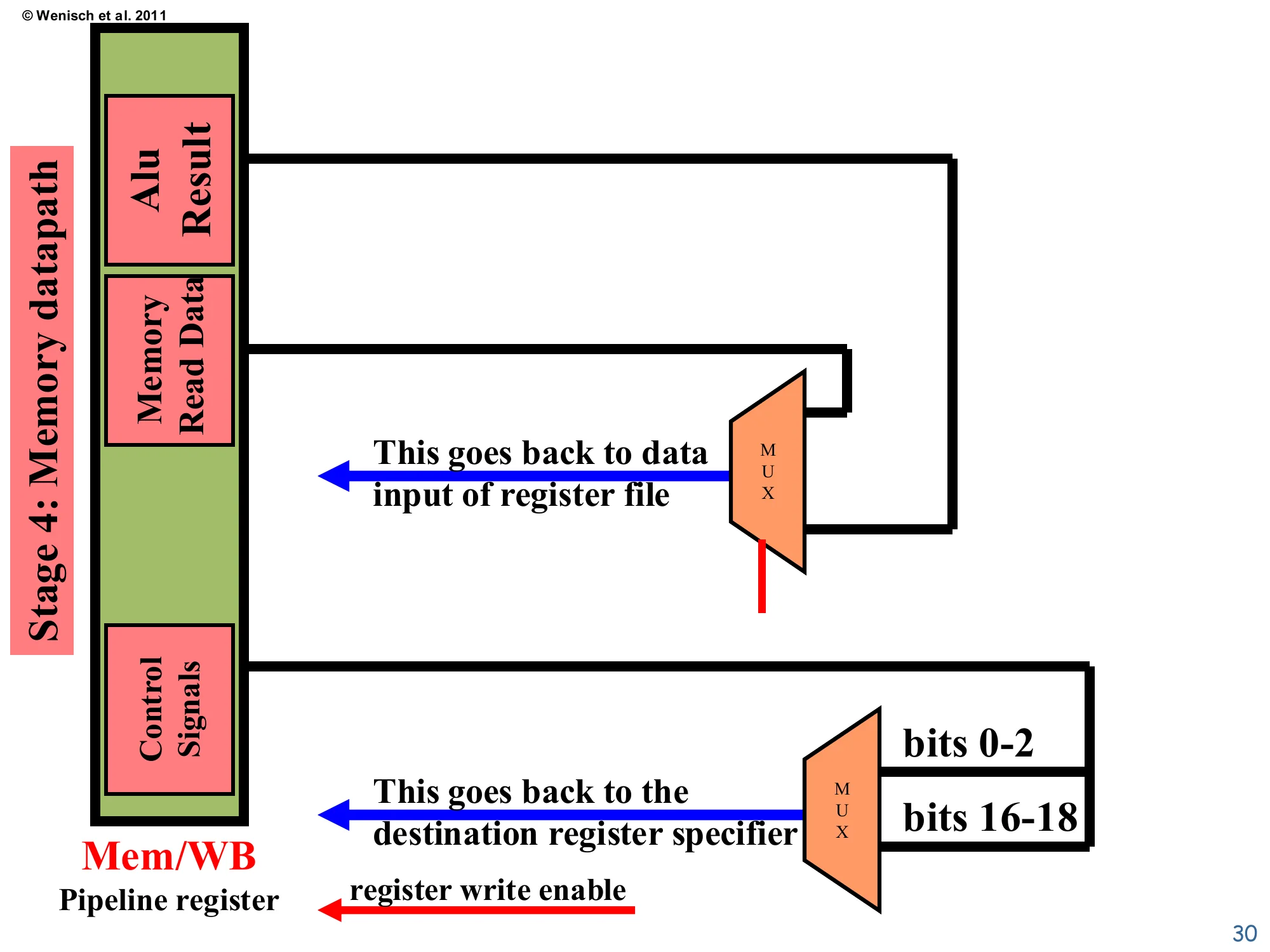
Show slide text
Write-back datapath
From Mem/WB: ALU Result, Memory Read Data, Control Signals.
A MUX selects between ALU Result and Memory Read Data → goes back to data input of register file. Another MUX selects between bits 0–2 and bits 16–18 of the instruction → goes back to the destination register specifier. A separate register write enable wire is driven from control signals.
The schematic finalizes the write-back loop. The data MUX picks the correct payload (ALU result vs. Memory Read Data) based on opcode, and that payload becomes the write-data input to the register file shown back in stage 2. A second MUX picks the destination-register specifier from one of two instruction-bit fields — different instruction formats place the destination register in different positions (R-type has dest in bits 16–18, while load/I-type uses bits 0–2 in this ISA encoding). The register write enable, also derived from the opcode, is what stops a store or branch from corrupting an arbitrary register. The two dotted feedback wires shown here close the picture: data flows back into the regfile’s data port, dest flows back into the regfile’s address port. Everything else is forgotten — once Write-back retires, the instruction’s pipeline state is gone.
Sample Code (Simple)
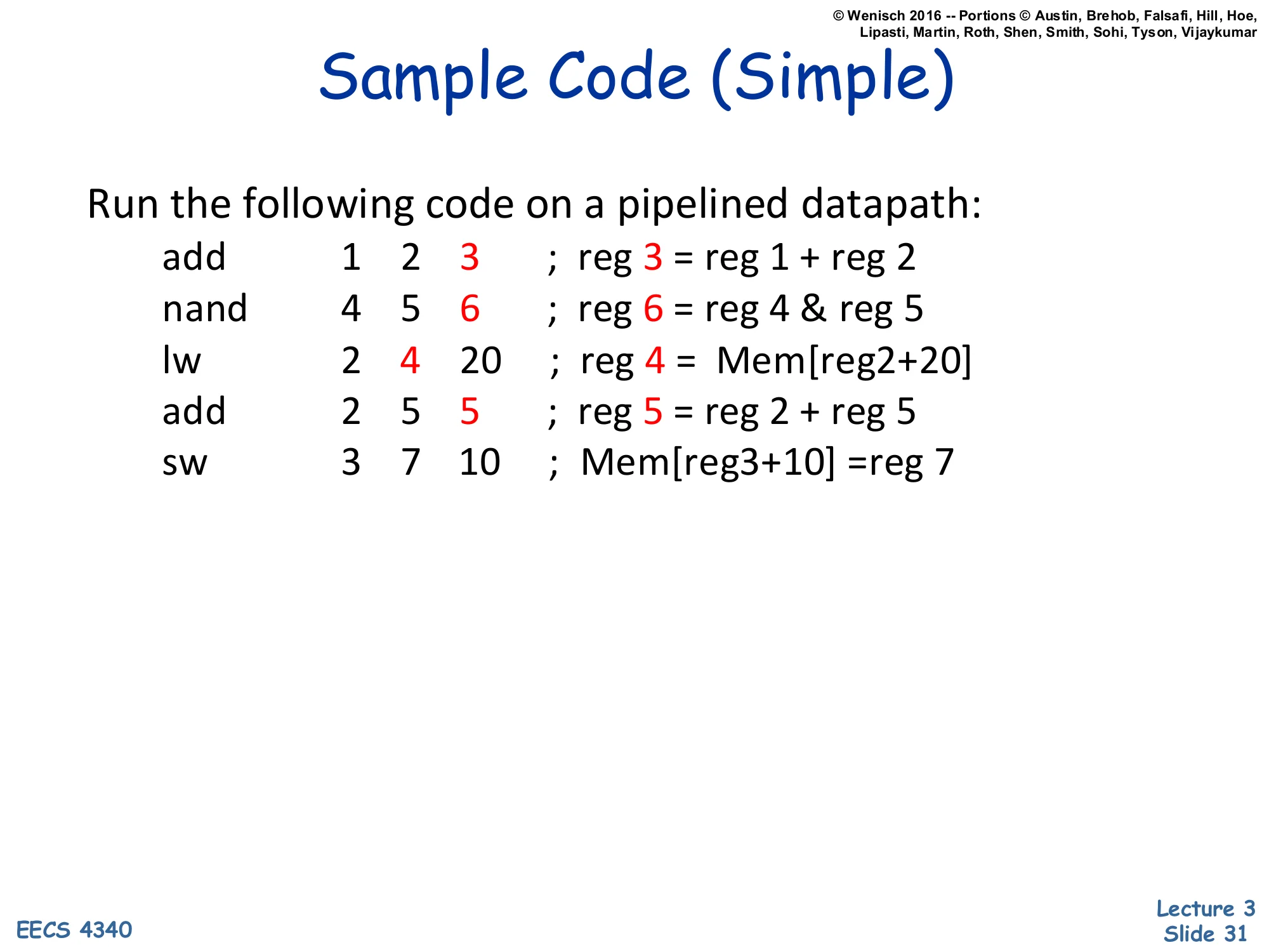
Show slide text
Sample Code (Simple)
Run the following code on a pipelined datapath:
| Instruction | regA | regB | dest/imm | Effect |
|---|---|---|---|---|
add | 1 | 2 | 3 | reg 3 = reg 1 + reg 2 |
nand | 4 | 5 | 6 | reg 6 = reg 4 & reg 5 |
lw | 2 | 4 | 20 | reg 4 = Mem[reg2+20] |
add | 2 | 5 | 5 | reg 5 = reg 2 + reg 5 |
sw | 3 | 7 | 10 | Mem[reg3+10] = reg 7 |
This five-instruction snippet is the running example for the next ten slides. It is deliberately simple: there are no RAW dependencies between back-to-back instructions, so no stalls or forwarding will be needed and we can watch the pipeline operate at peak throughput. (nand reads 4 and 5; the next lw reads 2 and 4, where 4 is the destination of nand — but the example assumes 4’s original value is what lw wants for its address calculation, which is what the slides show happening.) The mix covers all opcode classes: two arithmetic instructions, one nand-style logical, one load, and one store, exercising every stage of the datapath. The numerical traces on slides 33–42 show concrete values flowing through the pipeline at each clock edge so that you can verify your understanding of how each pipeline-register field is populated.
Annotated full pipeline datapath
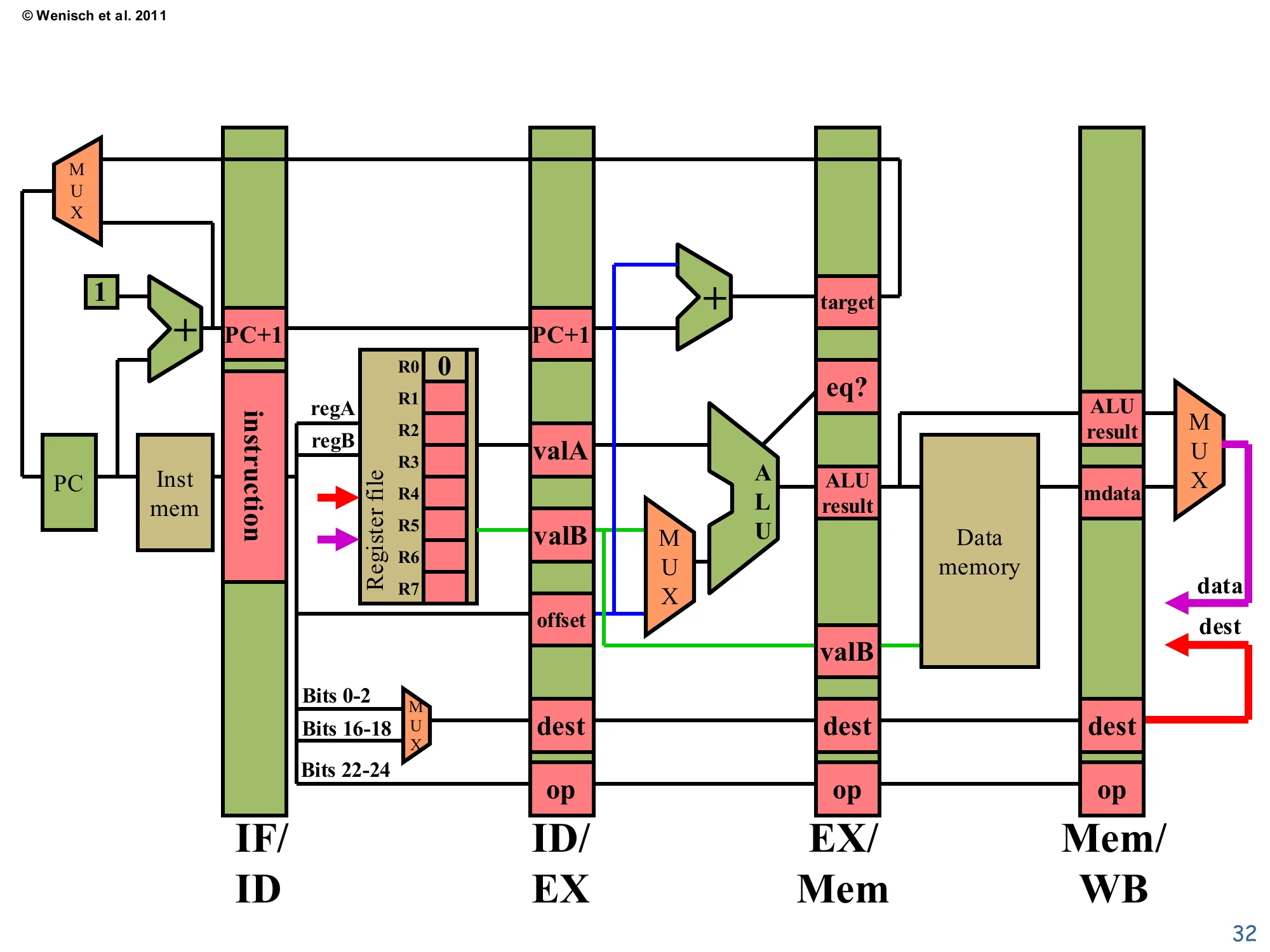
Show slide text
Annotated full pipeline datapath
Four pipeline registers (IF/ID, ID/EX, EX/Mem, Mem/WB) with named fields:
- IF/ID: instruction; PC+1
- ID/EX: PC+1, valA, valB, offset, dest, op
- EX/Mem: target, eq?, ALU result, valB, dest, op
- Mem/WB: ALU result, mdata, dest, op
Includes register-file read ports for regA, regB; one write port (data, dest, write-enable) fed back from Mem/WB.
This is the full annotated single picture of the 5-stage pipeline used as the reference for the simulation slides. Each pipeline register lists the fields it carries: IF/ID has the instruction bits and PC+1; ID/EX carries the decoded operands, immediate offset, destination index, and the opcode; EX/Mem adds the ALU result, branch target, and equality flag for branch resolution; Mem/WB carries either the ALU result or the load-returned mdata. The two MUXes on the bottom-right (after Mem/WB) are the same write-data and write-dest MUXes from slide 30. The register-write-enable wire is the red arrow at the very bottom. Keep this picture in mind for the eight cycle-by-cycle traces that follow — each trace just colors in numerical values for the fields listed here.
Initial State (Cycle 0)
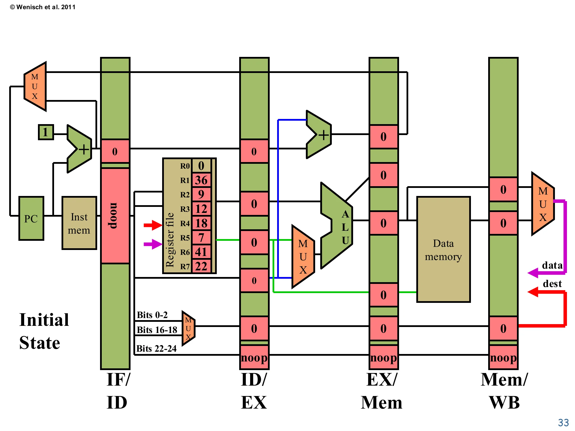
Show slide text
Initial State
Register file contents: R0=0, R1=36, R2=9, R3=12, R4=18, R5=7, R6=41, R7=22.
All pipeline registers hold 0 / noop. PC=0.
Before instruction execution begins, every pipeline register is initialized to a noop: data fields are zero and the opcode field carries the special noop encoding so that downstream stages take no architectural action. The register file is preloaded with the values shown so the trace produces concrete numbers on subsequent cycles. PC is at 0, ready to fetch the first instruction. The empty pipeline reflects the fill phase: until the first instruction reaches Mem/WB at cycle 5, fewer than five instructions are in flight, so throughput is below the steady-state limit. Conversely, after the last instruction enters Fetch (cycle 5 here), the pipeline starts to drain, again at less than peak throughput. For long programs these fill and drain costs amortize away; for short programs they matter, and they are exactly what limit speedup in tight loops with branches.
Time 1: Fetch add 1 2 3
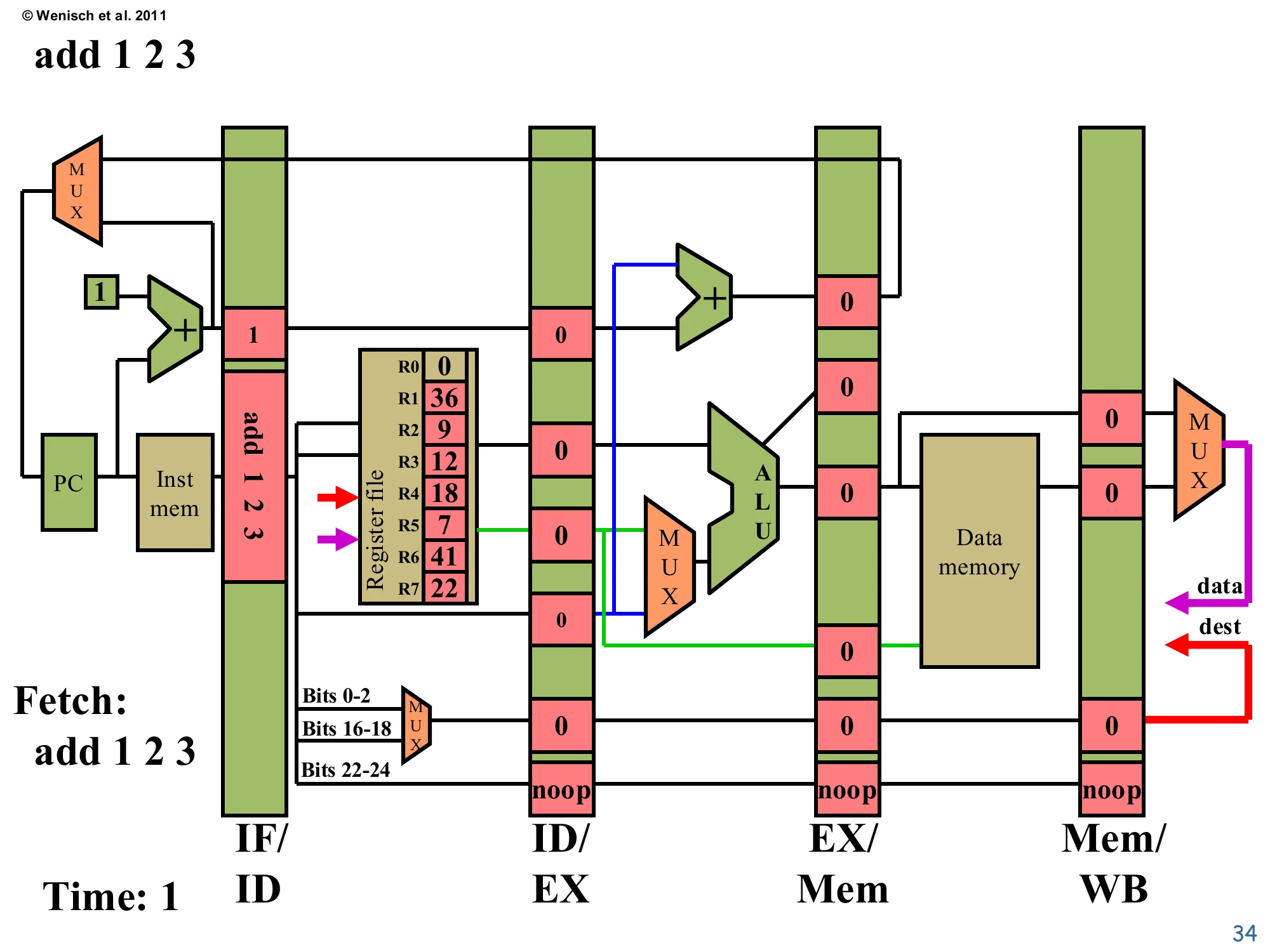
Show slide text
Time: 1 — Fetch: add 1 2 3
IF/ID now holds: instruction = add 1 2 3, PC+1 = 1.
ID/EX, EX/Mem, Mem/WB still hold noop / 0.
On the first edge after reset, Fetch reads the first instruction (add 1 2 3) from instruction memory and latches it, along with PC+1 = 1, into IF/ID. The PC register itself updates to 1 in preparation for next cycle’s fetch. All later pipeline registers still hold their initial noop values because no instruction has reached them yet. This is the simplest cycle in the trace — only stage 1 is doing useful work, and the other four stages are idle, propagating noops forward. Notice how the PC’s MUX selects the +1 path (no branch is in flight to override it). On the very next cycle, two stages will be active: Fetch on nand and Decode on add.
Time 2: Fetch nand 4 5 6, Decode add
Show slide text
Time: 2 — Fetch: nand 4 5 6 (add 1 2 3 in Decode)
IF/ID: instruction=nand 4 5 6, PC+1=2.
ID/EX (for add): PC+1=1, valA=36 (R1), valB=9 (R2), offset=3, dest=3, op=add.
Now two stages are active. nand 4 5 6 is fetched and latched into IF/ID with PC+1=2. Simultaneously, the previous-cycle’s add 1 2 3 reaches Decode, which reads R1=36 and R2=9 from the register file and populates ID/EX with valA=36, valB=9, dest=3, opcode=add. The destReg MUX in Decode picks bits 0–2 of the instruction (red font in the diagram) — that’s the add’s destination-field encoding. The opcode threaded through ID/EX is add, so the next cycle’s Execute will route valB (not the offset) into the ALU. This second cycle marks the beginning of pipelining benefit: two instructions are in flight, doubling the work being done per clock relative to a non-pipelined design.
Time 3: Fetch lw, Decode nand, Execute add
Show slide text
Time: 3 — Fetch: lw 2 4 20
IF/ID: instruction=lw 2 4 20, PC+1=3.
ID/EX (for nand): valA=18 (R4), valB=7 (R5), offset=6, dest=6, op=nand.
EX/Mem (for add): ALU=45 (= 36+9), valB=9, target=4 (=PC+1+offset, branch adder result), dest=3, op=add.
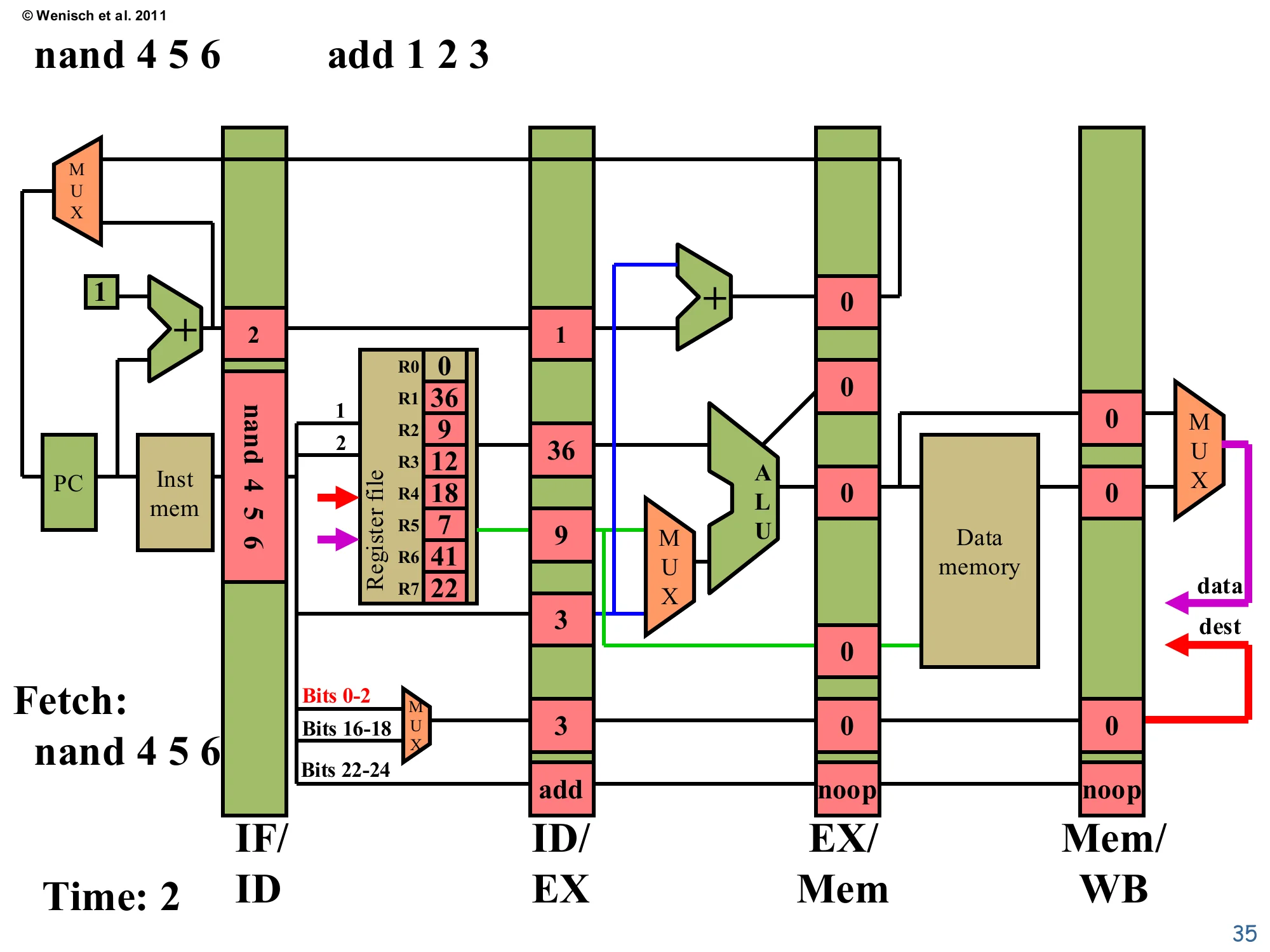
Three instructions in flight. lw 2 4 20 is fetched (PC+1=3). nand 4 5 6 decodes to valA=R4=18, valB=R5=7, dest=6. add 1 2 3 executes: the ALU adds 36+9=45, the branch adder produces PC+1+offset=4 (irrelevant for an add), and the result lands in EX/Mem. The destReg field of EX/Mem now holds 3 (the destination of add), waiting to be written in two more cycles. Notice the dest specifier MUX is selecting bits 0–2 (highlighted red), the encoding for the nand’s destination index in ID/EX. This is steady-state pipelining at three instructions per cycle of work — the throughput benefit is real and growing as more stages fill.
Time 4: Fetch add 2 5 5, four instructions in flight
Show slide text
Time: 4 — Fetch: add 2 5 5
IF/ID: instruction=add 2 5 8(annotated; coded as add 2 5 5), PC+1=4.
ID/EX (for lw): valA=9 (R2), valB=18 (R4 — not used as data, lw uses offset), offset=20, dest=4, op=lw.
EX/Mem (for nand): ALU = 18 NAND 7 = -3, valB=7, target=8, dest=6, op=nand.
Mem/WB (for add): ALU=45, mdata=0, dest=3, op=add.
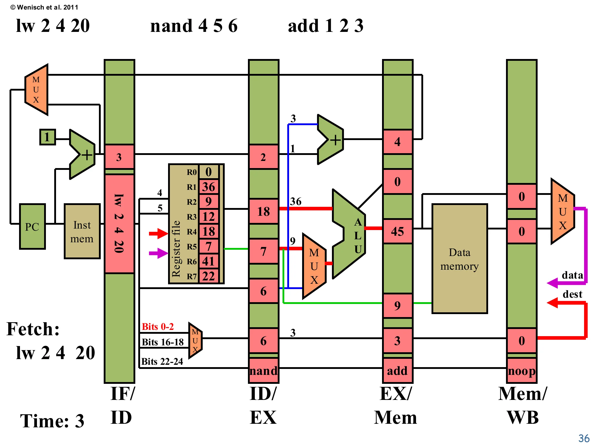
Four instructions are now active. The add 2 5 5 is being fetched. lw 2 4 20 decodes to valA=R2=9, dest=4, offset=20, opcode=lw — the destReg MUX flips to bits 16–18 (highlighted red) because lw encodes its destination differently than R-type. nand 4 5 6 executes: the ALU computes 18 NAND 7 = -3 (in two’s complement with 18=10010 and 7=00111, NAND yields 11111111…101 = -3 as signed). Most importantly, add 1 2 3 reaches Mem/WB carrying ALU=45, dest=3, op=add — this means in the next cycle the register file will be written with R3=45. The pipeline is at peak utilization: every stage is doing real work simultaneously, which is the entire point of pipelining.
Time 5: Fetch sw, all five stages active
Show slide text
Time: 5 — Fetch: sw 3 7 10
IF/ID: instruction=sw 3 7 10, PC+1=5.
ID/EX (for add 2 5 5): valA=9 (R2), valB=7 (R5), offset=4, dest=5, op=add.
EX/Mem (for lw): ALU=29 (=9+20), valB=18, target=23, dest=4, op=lw.
Mem/WB (for nand): ALU=-3, mdata=0, dest=6, op=nand.
Register file: R3 has been written to 45 (highlighted green) — write-back of the original add.
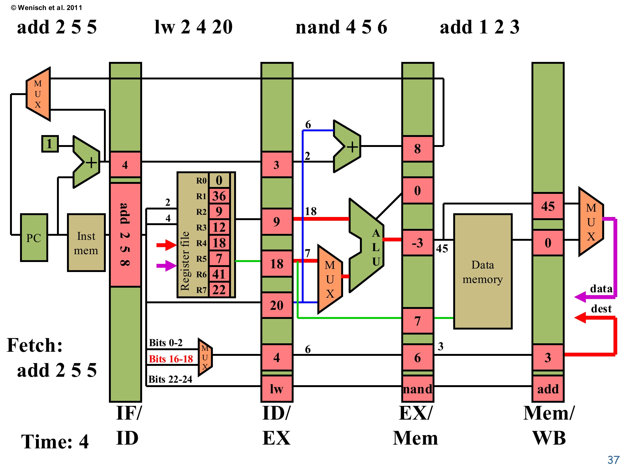
All five stages are simultaneously active — the pipeline is at full throughput. The original add 1 2 3 retired this cycle: R3 was updated to 45 (highlighted green). nand is in Memory; since it’s not a load or store, the D-cache is disabled and its ALU result -3 just propagates through. lw 2 4 20 is in Execute and computes its address: 9 + 20 = 29 (its ALU result). add 2 5 5 is in Decode reading R2=9 and R5=7. sw 3 7 10 is being fetched. From this cycle until the pipe drains, one new instruction completes write-back per clock — the canonical pipelined result of CPI ≈ 1 even though each individual instruction still takes 5 cycles end-to-end.
Time 6: Pipeline draining begins
Show slide text
Time: 6 — No more instructions to fetch
IF/ID: empty (no more instructions).
ID/EX (for sw): valA=R3=45 (green; just written last cycle), valB=R7=22, offset=10, dest=7, op=sw.
EX/Mem (for add 2 5 5): ALU=16 (=9+7), valB=7, target=9, dest=5, op=add.
Mem/WB (for lw): ALU=29, mdata=99, dest=4, op=lw.
Register file: R6 written to -3 (green) — nand retired.
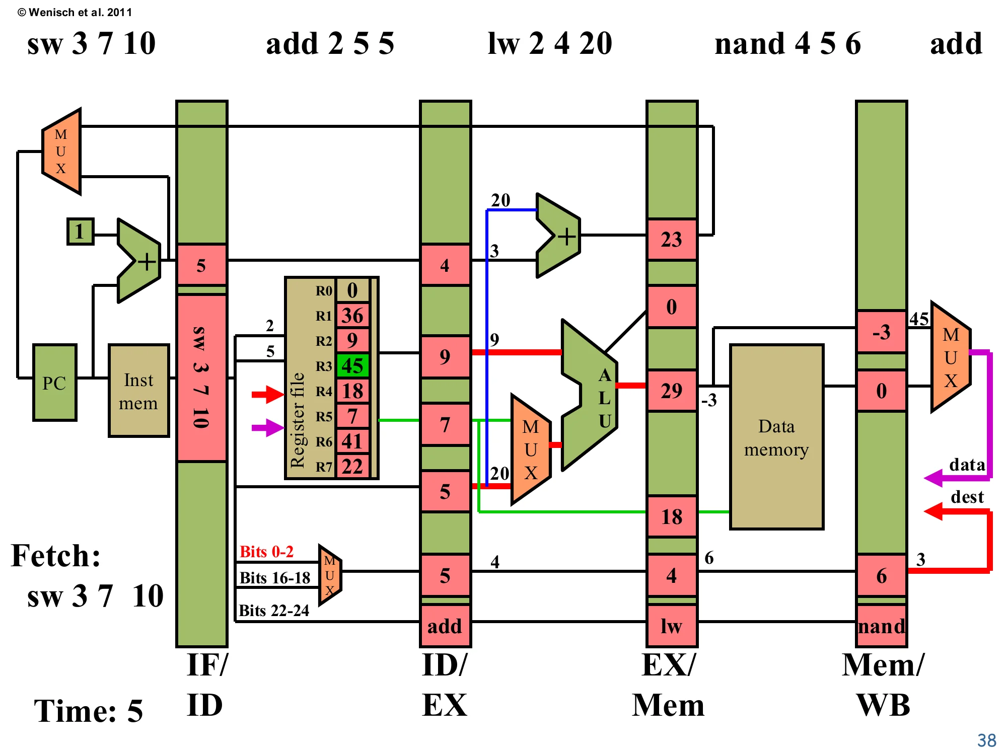
The fetch stream has ended (no more instructions), so IF/ID begins to fill with noops. nand’s write-back fired, putting R6 = -3 (green) into the register file. lw finishes Memory: ALU=29 was the address, and the D-cache returned mdata=99 — that’s the value that will be written into R4 when lw retires. add 2 5 5 executes: 9+7=16. sw 3 7 10 decodes — note that R3=45 (green) is just read this cycle, the value that was written one cycle earlier; this works because the register-file write-port commits in the first half of the cycle and the read port samples in the second half (or because forwarding is in place — see L04). This example sidesteps a true RAW hazard because the values produced by add 1 2 3 and nand 4 5 6 are not consumed by adjacent instructions.
Time 7: lw write-back
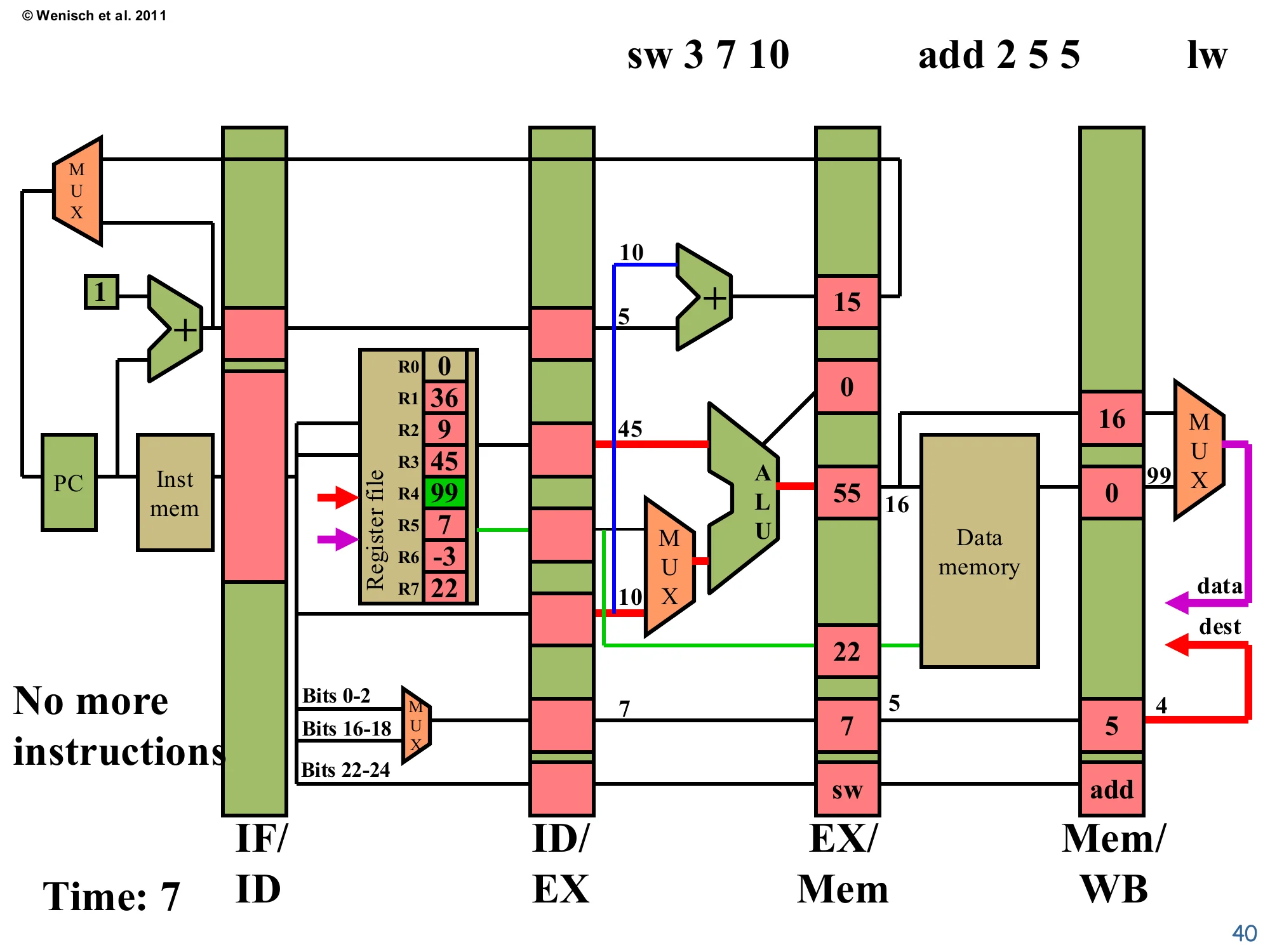
Show slide text
Time: 7 — sw 3 7 10 in Execute
No more instructions to fetch.
EX/Mem (for sw): ALU=55 (=45+10), valB=22, target=15, dest=7, op=sw.
Mem/WB (for add 2 5 5): ALU=16, mdata=0, dest=5, op=add.
Register file: R4 written to 99 (green) — lw retired.
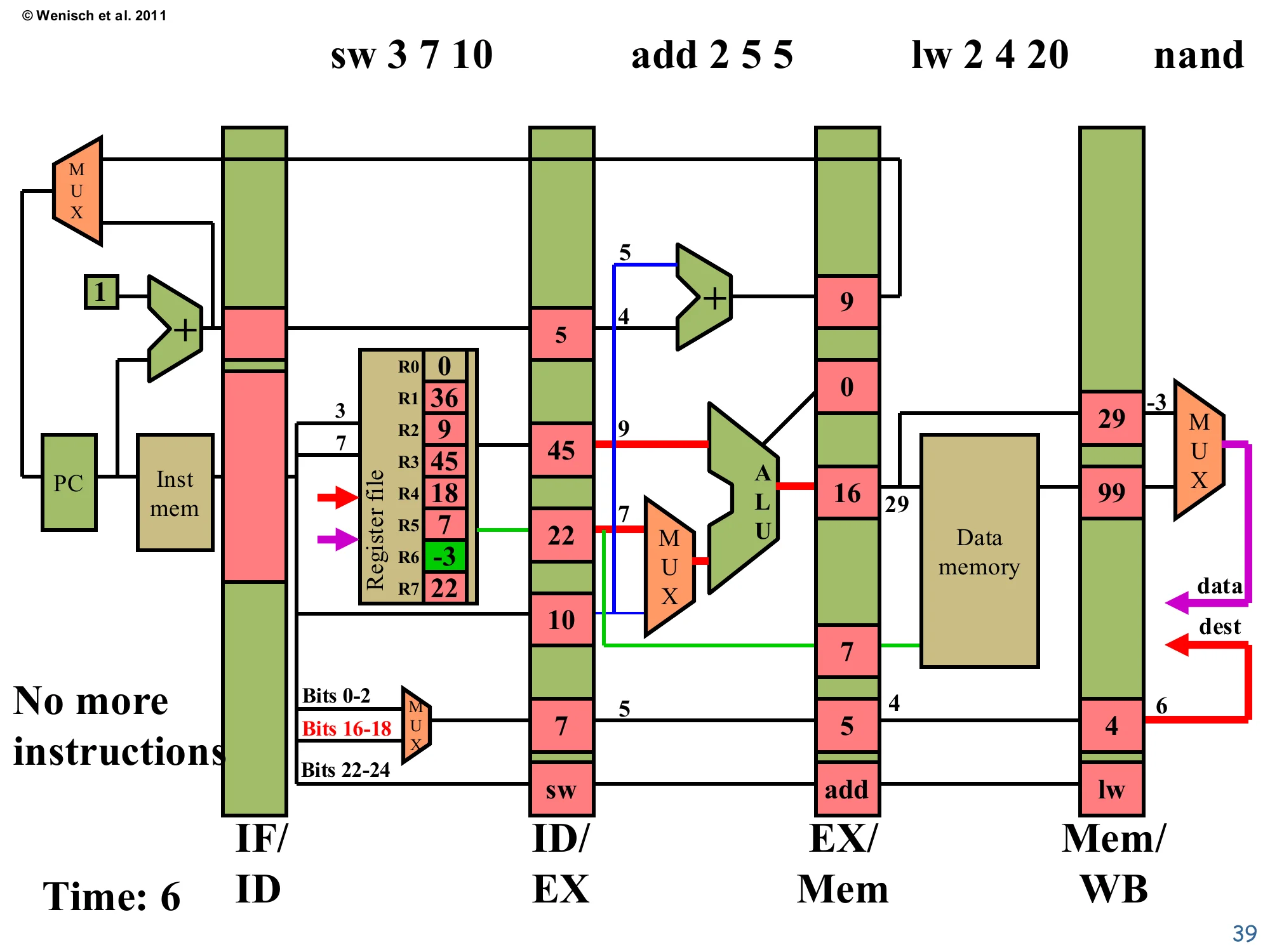
lw retires: R4 receives the loaded value 99 (green). add 2 5 5 finishes Memory (no cache access — arithmetic op) and arrives in Mem/WB. sw 3 7 10 is in Execute, where the ALU computes the store address as R3 + 10 = 45 + 10 = 55. The valB field carries 22 = R7, the data value that the store will write next cycle. Two pipeline slots are now empty (noop) ahead of sw because there are no more instructions, so throughput is below peak again — this is the drain phase symmetric to the fill at the start of the trace. Real programs minimize drain time by never letting the pipeline run dry, but program tail-ends and tight loops with mispredicted branches both incur drain costs.
Time 8: sw memory access
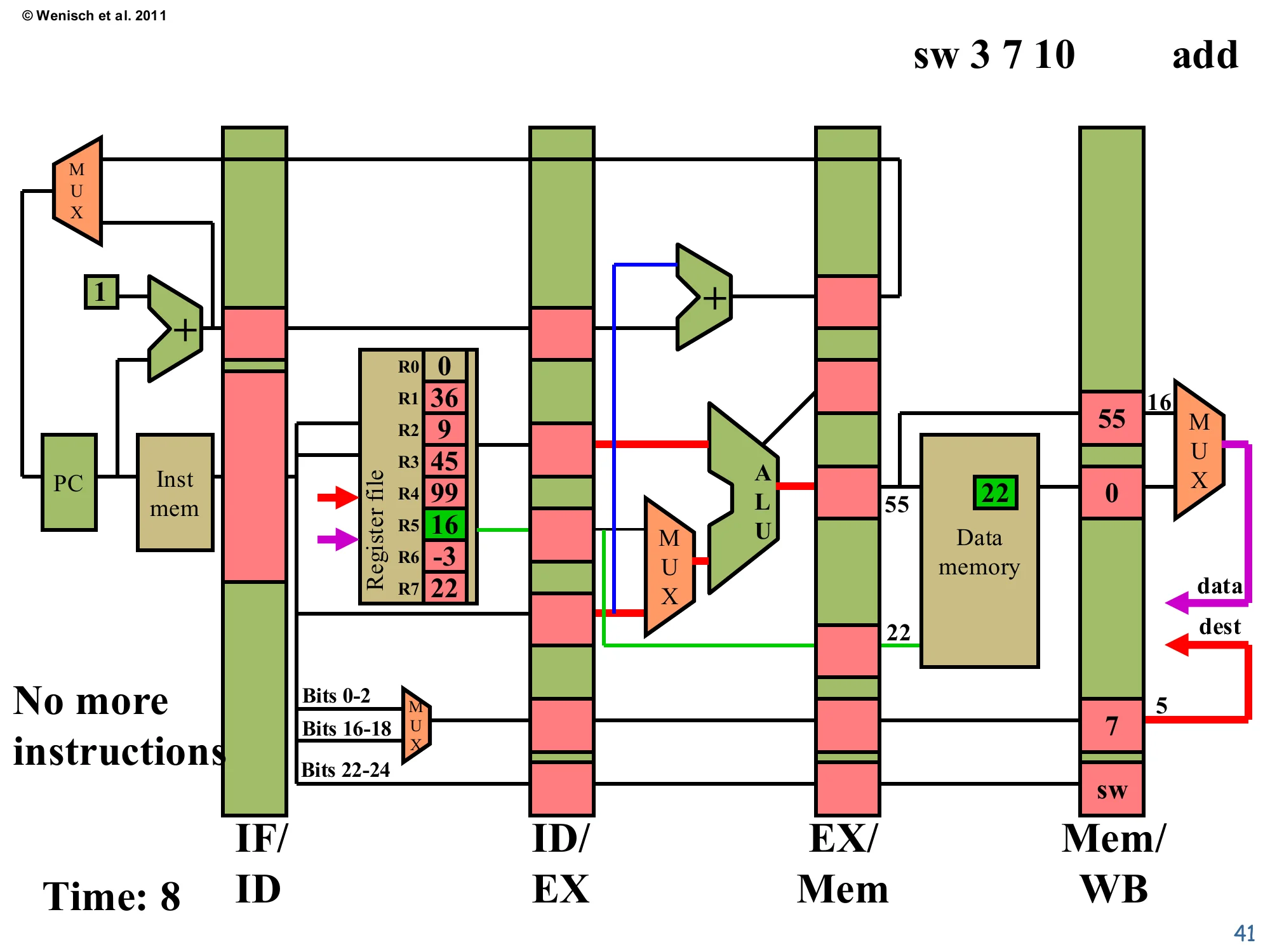
Show slide text
Time: 8 — sw 3 7 10 in Memory
Mem/WB (for sw): no register write — just propagating control.
Data memory: address 55 receives 22 (green box).
Register file: R5 written to 16 (green) — second add retired.
add 2 5 5 retires: R5 = 16 (green). sw reaches Memory and writes its data. The Data Memory cell at address 55 now holds 22 (highlighted green) — that is the architectural side-effect of the store. The Mem/WB pipeline register downstream still carries the sw’s control signals, but the destReg write-enable will be 0 (stores don’t write any register), so the write-back stage simply discards it. Notice the target field in EX/Mem is empty — sw produces no value to feed back as a branch target. Only one instruction is left in the pipeline now, ready to drain through Write-back next cycle.
Time 9: sw write-back (no register write)
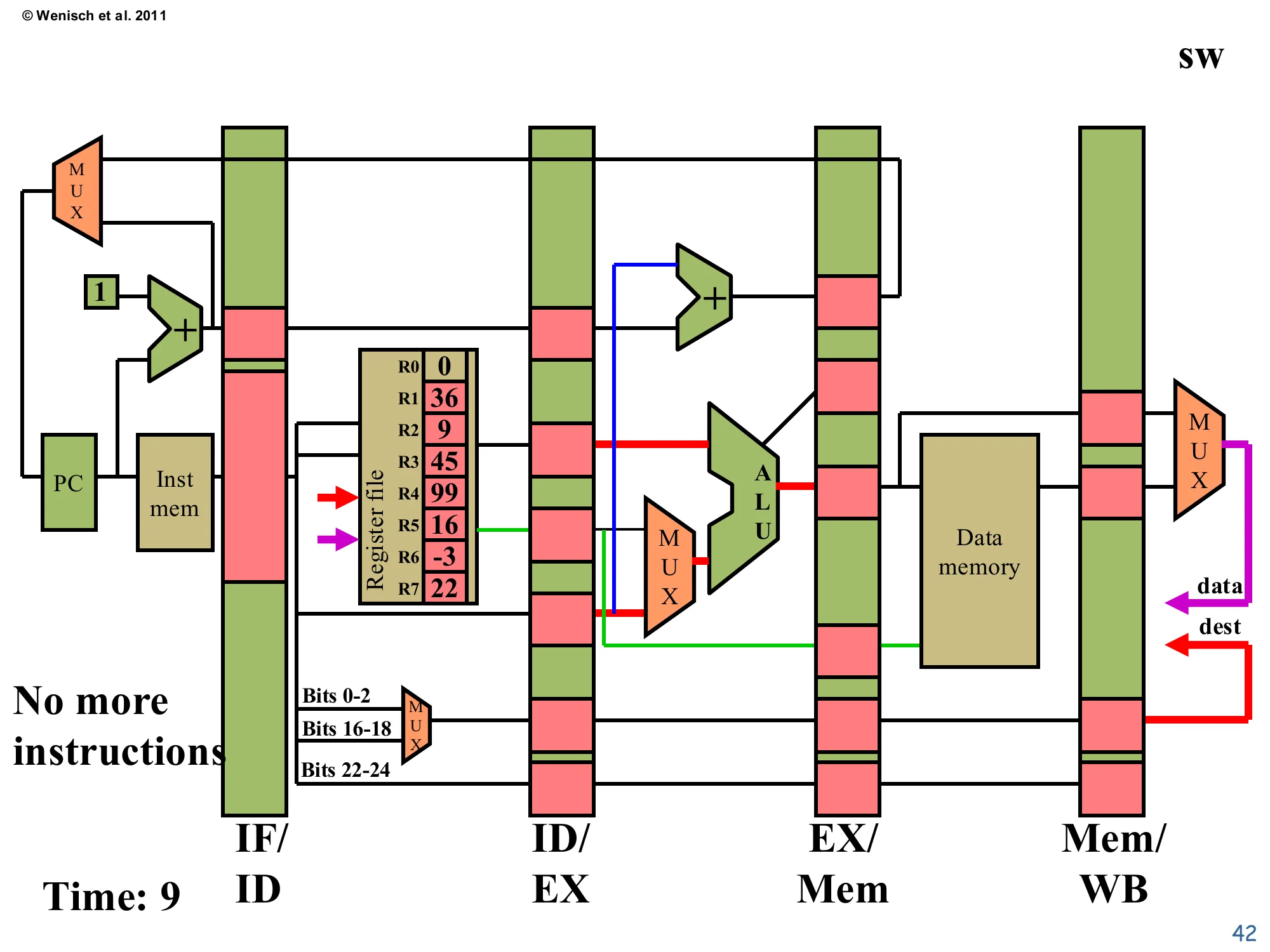
Show slide text
Time: 9 — sw in Write-back
No more instructions in flight after this cycle.
Register file final state: R0=0, R1=36, R2=9, R3=45, R4=99, R5=16, R6=-3, R7=22.
sw reaches Write-back, but stores don’t update any register, so the write-enable is deasserted and the register file is unchanged. The pipeline is now drained. The final architectural state reflects every committed instruction’s effect: R3 was updated by add 1 2 3, R6 by nand, R4 by lw (loaded from memory), R5 by add 2 5 5, and Mem[55]=22 by sw. Total elapsed time: 9 cycles for 5 instructions — a CPI of 9/5 = 1.8 for this short trace because of fill and drain overhead. In steady state on a long program, the same pipeline asymptotes to CPI = 1 (one new instruction retiring per cycle), confirming the headline benefit of pipelining.
Time graphs
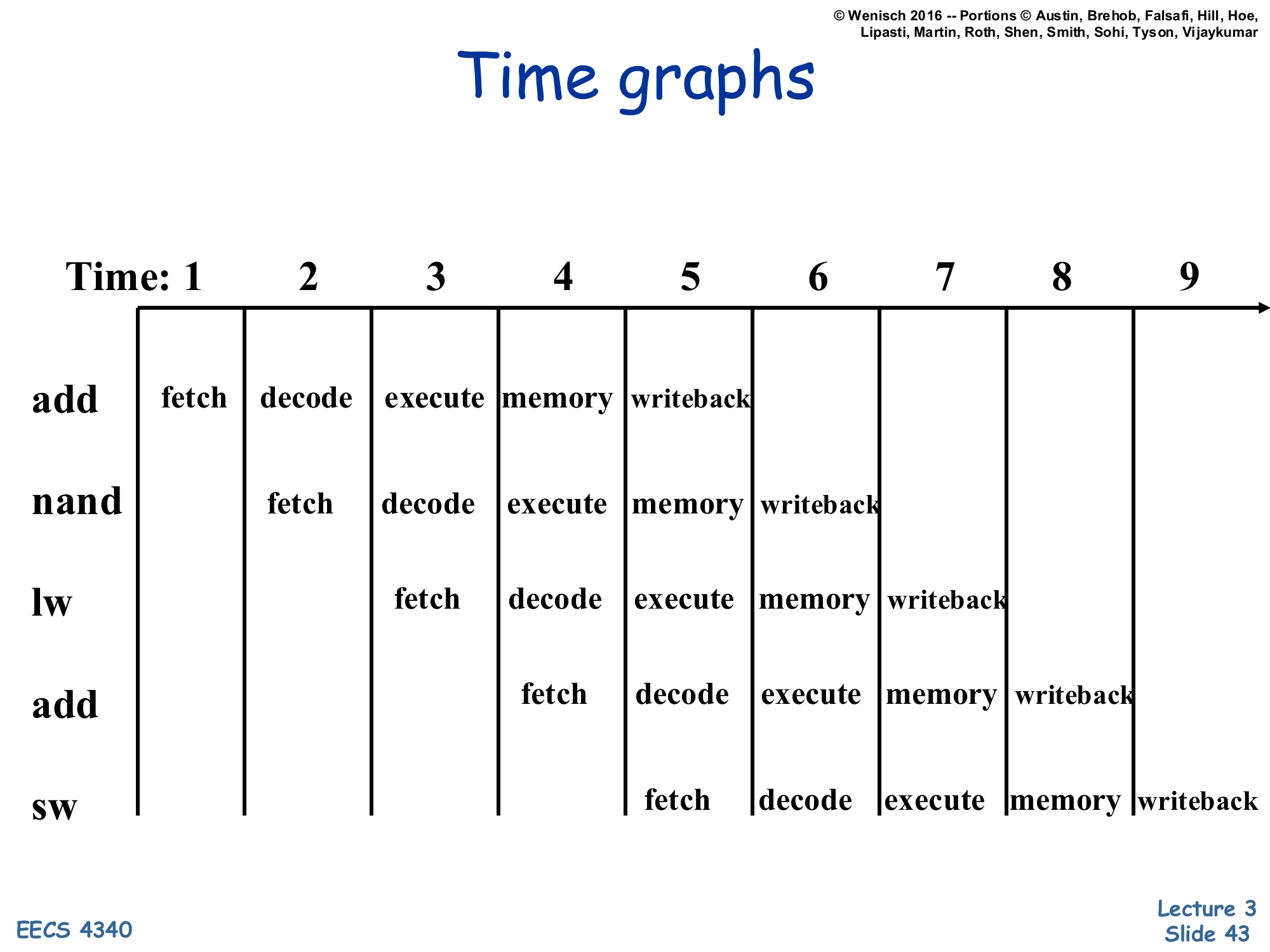
Show slide text
Time graphs
| T1 | T2 | T3 | T4 | T5 | T6 | T7 | T8 | T9 | |
|---|---|---|---|---|---|---|---|---|---|
| add | fetch | decode | execute | memory | writeback | ||||
| nand | fetch | decode | execute | memory | writeback | ||||
| lw | fetch | decode | execute | memory | writeback | ||||
| add | fetch | decode | execute | memory | writeback | ||||
| sw | fetch | decode | execute | memory | writeback |
The space-time diagram is the standard textbook way to summarize a pipeline trace. Each row is one instruction, each column is one cycle, and each cell is the stage that instruction occupies that cycle. The diagonal stripe pattern is the fingerprint of an unstalled in-order pipeline: one new fetch per cycle, instructions descending one stage per cycle, and the last instruction retiring four cycles after fetch begins. The total cycle count for N instructions through a k-stage pipeline is N+k−1 (here 5+5−1=9), so steady-state CPI tends to 1 only in the limit N≫k. Hazards (RAW, structural, control) introduce stalls that show up as repeated stages — the same stage occupied by the same instruction across multiple cycles — or as bubbles inserted between instructions; those will be the focus of L04.
Balancing Pipeline Stages — Speedup analysis
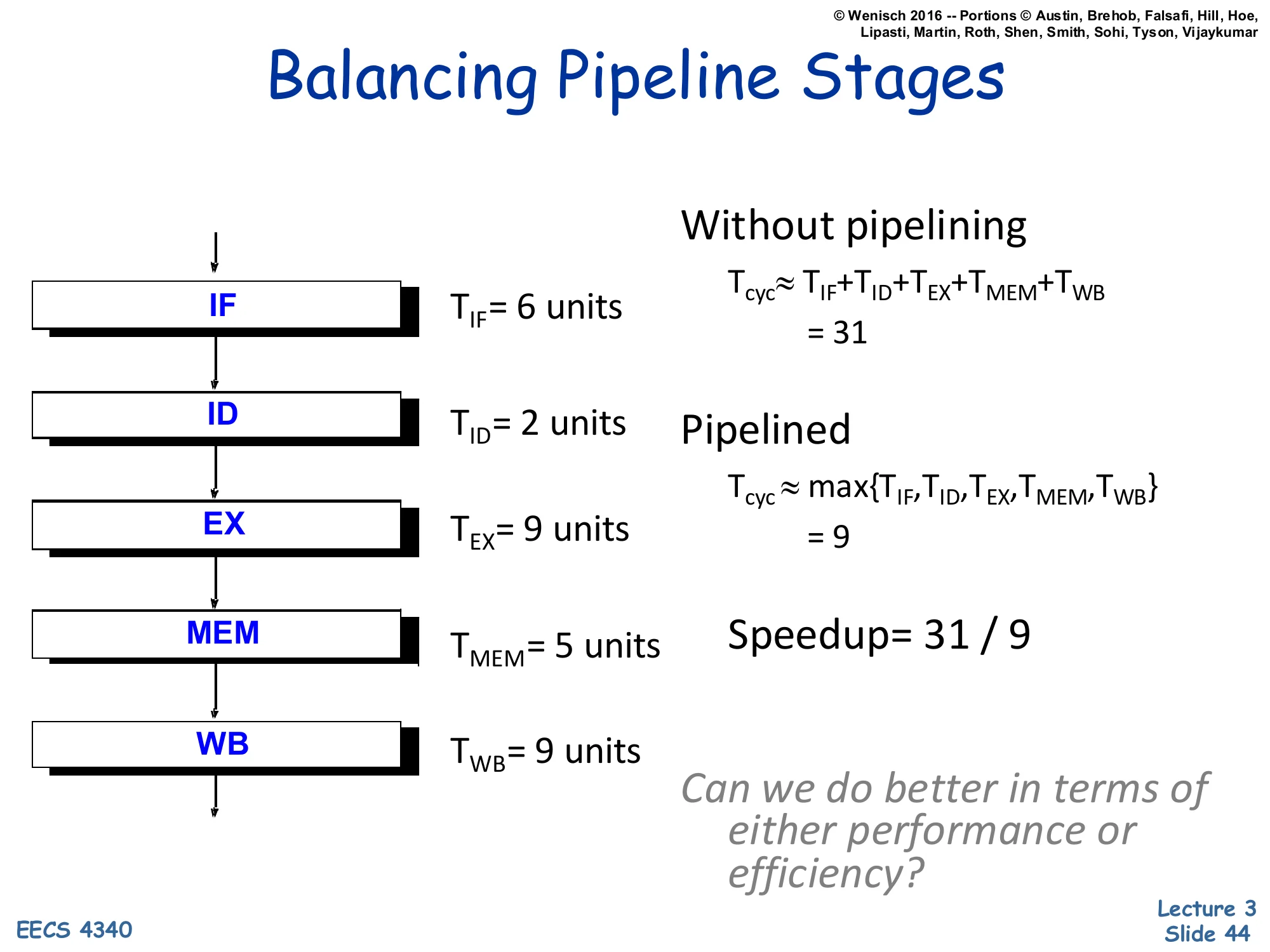
Show slide text
Balancing Pipeline Stages
- TIF=6 units
- TID=2 units
- TEX=9 units
- TMEM=5 units
- TWB=9 units
Without pipelining: Tcyc≈TIF+TID+TEX+TMEM+TWB=31
Pipelined: Tcyc≈max{TIF,TID,TEX,TMEM,TWB}=9
Speedup = 31 / 9
Can we do better in terms of either performance or efficiency?
This slide makes the speedup arithmetic concrete. Sum the per-stage delays for the unpipelined critical path: 6+2+9+5+9 = 31 units. Pipelined, the cycle is set by the slowest stage, so Tcyc=max(6,2,9,5,9)=9 units. Speedup is 31/9≈3.4× — short of the theoretical 5× because the stages are not balanced: ID at 2 units is far below the 9-unit max, so 7 of every 9 units in that stage are wasted slack. The closing question previews the next slide: by either merging under-utilized stages (combining ID with another) or subdividing the slow stages (splitting EX or WB into halves), the design can push closer to the ideal 5× — but the trade-off is more pipeline registers, more hazards, and longer branch-mispredict penalties.
Balancing Pipeline Stages — methods and trends
Show slide text
Balancing Pipeline Stages
Two Methods for Stage Quantization:
- Merging of multiple stages
- Further subdividing a stage
Recent Trends:
- Deeper pipelines (more and more stages)
- Pipeline depth growing more slowly since Pentium 4. Why?
- Multiple pipelines (subpipelines)
- Pipelined memory/cache accesses (tricky)
Two complementary techniques rebalance the pipeline. Merging combines stages whose delays are short relative to the slowest, freeing pipeline-register area and reducing hazard windows. Subdividing splits a slow stage into two faster sub-stages — this is the classic deepening technique that took Intel’s Netburst (Pentium 4) to 20+ stages and a clock frequency of 3+ GHz. The slide flags that depth growth has slowed since Pentium 4, and the rhetorical “Why?” points at the well-known reasons: (1) latch overhead (setup, hold, clock-to-Q) becomes a non-trivial fraction of each shorter stage, eroding the bandwidth gains shown back on slide 19; (2) deeper pipelines amplify branch-mispredict penalties, eating throughput for any code with hard-to-predict branches; and (3) deeper pipelines burn more dynamic power per instruction because more flops toggle. Modern designs instead pursue width (multiple pipelines, superscalar) and pipelined cache accesses to keep memory’s long latency from dominating.
Readings (closing)
Show slide text
Readings
For today:
- H & P Chapter C.1–C.4
Announcements (closing)

Show slide text
Announcements
- Lab #2 this Wednesday
- Please bring your computer
- Involve graded assignments
- Attendance is required and graded
- Project #1
- Due 4-Feb-26
- Project #2
- Will be released today (2-Feb-26)
- Due 11-Feb-26
- More details in the lab